This thread has been locked.

If you have a related question, please click the "Ask a related question" button in the top right corner. The newly created question will be automatically linked to this question.

TPS3619: TPS3619-33 overdrawing current at the VBAT path after a few runs

Part Number: TPS3619


Hello,

We've been having a few problems in integrating the TPS3619-33 into a product we've been working on successfully. Right now after installing a new TPS3619 into our board , after a few hookups at the Vbat input with a variable bench linear power supply the IC tends to over draw current, bearing in mind that if the current was not limited by the power supply the IC would definitely burnout ( right now limited to 10mA and unfortunately it is maxed out) and I've disconnected the load and it is clear now the TPS3619 is the one drawing the current. At this state the IC can still switch between Vbat and VDD automatically, but it is clear that it is not advised to continue using the IC in this state and a replacement is required, but I would really appreciate if someone would advise what would cause this behaviour.
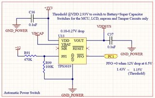
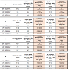
VBAT : 3.0-3.6V

VDD : 3.2-3.3V

What i have in mind of possible suspects ,

1. ESD , maybe VBAT needs an ESD diode ?.

2. PFO is directly connected to the MCU GPIO (0 - 3.3V) , I'm not sure maybe some condition that may fry the IC ?

3.  The bench power supply connectors arcing or overshooting maybe during power on/off at the VBAT input ? (Siglent  SPD3303X-E ).

Regards

Omar Sultan

  • Hi Omar,

    When you say the IC is drawing current, is the current going into the VDD pin?  Do you have separate power supplies for the VBCAP and for the 12V rail?  My suggestion is to try and disconnect everything (output load, /PFO, and ground the PFI input) and see if the TPS3619 is consuming current.  Your schematic looks okay and I dont see anything that suggest it is hooked incorrectly.  

    Have you checked the pins to see if there is a "soft" short somewhere on your PCB board?  Try using an ohmmeter and see if there are any ohmic readings that do not look correct.  

    Ben

  • Hello Ben,

    Thank you for the quick response. No the current drawn  is through VBAT even if VDD is powered on (overdrawn 10->100mA) but i'm having it limited by the Power supply. So if VDD is present VBAT is drawing the huge current , when VDD is not present VBAT is still chomping on the sweet current.


    Yes Both separate; VBCAP is the Battery but in this test case Power supply , and the 12V is coming from a separate Ac/dc power supply. 12V supplies the LDO that gives out VDD.

    I've tried disconnecting the load and still same current drawn by the IC itself . I've yet to try and disconnect the PFO, PFI as well and the load with it. But if something changes .... currently do you have an idea on the suspected cause ?

    I'm not sure i understand of the term "soft short" i apologise , but i'd like to note that the IC works fine for "some" time on some boards and others may act up sooner. ( I have several boards assembled ).

    BR


  • Hi Omar,

    What voltage is VDD?  Is (VDD > VIT-)?  In order for VBAT to not be connected to the output via 15-ohm PMOS switch, is VDD must be greater than 2.93 + Vhys, where Vhys = 40mV (typ).  

    Did you try a new part?  From the sounds of your explanation, the part maybe damaged.  I would try and disconnect the PFO, PFI and the load so you can isolate the problem that you are seeing.

    Soft short means there is some resistance but not a hard short where the resistance is almost 0 ohms.

    Seems like you may have soldering issue?

    Ben

  • Hello Ben,

    VDD is 3.2V and  yes it is greater than VIT .  Yes after installing a new and working TPS3619-33 everything works as expected ; VBAT does not open rail while VDD is greater than VIT- , The problem does not happen until after a while of operation of the circuit as mentioned in the first post where eventually VBAT rail is drains alot of current in both cases ( VDD > VIT ) or vice versa.

    Yes I am positive the part gets damaged and i've replaced plenty and they work for a while then go bad after a while of usage by using a bench linear power supply (variable output) at the VBAT input. I can try ad disconnect the PFI , PFO and Load on the damaged part and see if it still draws alot of current.

    Ok thank you for explaining the term of "soft short" but can you explain which pins of the TPS3619 do i need to check of soft shorts ?

    I doubt a soldering issue in terms of colder solder or shorts, maybe if you mean in terms of exposing the IC to high termperatures over an extended time maybe but i doubt it.

    BR

  • Hi Omar,

    I am very curious after some time of operation the part seems to damage itself.  I seems that the current is going through the TPS3619 and out of the GND pin. I really dont have an explanation of why the part is damaging itself after a period of time.  Can you limit the Bench Linear power supply (variable output) output current to 1mA going into the VBAT pin?  When you do this, does the part still get damaged?  You mentioned that there is no load during your test, right?  Just be careful of the amount of current that is going into the VBAT pin. The PMOS switch is 15-ohms and if you running 10mA, that is 150mW of power that is going through the IC.

    With the failed units, can you measure the resistance between VBAT and GND? VBAT to VDD?  By doing this, it might give us a clue about the VBAT pin.  

    Ben

  • Hello Ben,

    I've disconnected PFI , PFO and the Load off of theTPS3619-33 IC and still it draws alot of current ( The damaged one installed right now is drawing for itself on the VBAT line around 0.18A ). Unfortunately my power supply can limit starting from 10mA. 

    I have other boards which have the IC replaced and then set aside so they are healthy and working fine (tested once only) , so below as per requested i've measured the resistance on both working and damaged boards,

    A. Damaged Board:

    - Resistance of VBAT <-> GND = 560 ohms.

    Resistance of VDD <-> GND = 400 ohms.

    - Resistance of VOUT <-> GND = 12.8K - 13K ohms

    - Resistance of VDD <-> VBAT = 810 - 948 ohms.

    B. Working Board (tested once as working and then set aside):

    - Resistance of VBAT <-> GND = 26.8K - 27.5K ohms.

    Resistance of VDD <-> GND = 400 ohms.

    - Resistance of VOUT <-> GND = 12.8K - 13K ohms

    - Resistance of VDD <-> VBAT =27.4K - 28K ohms.

    BR

  • Hi Omar,

    It seems that the VBAT resistance is much lower when the part is damaged.  Can you add an inline resistor from the power supply to VBAT?  As long as VDD is less than VIT-, VBAT will show up on VOUT.  I would also add an ammeter to monitor the current going in the VBAT pin.  My hunch is that there is too much current going into the VBAT pin and causing the PMOS device to be damaged, based on the measured resistance you provided.

    Ben

  • Hello Ben,

    Would you kindly recommend a specific resistor value ? our application would need at peak 40mA for a few milliseconds then drop down to 725uA  for the rest of the application. Also If i understand this correctly the recommendation for installing the inline resistor is a solution or is it just to further diagnose the problem ?

    BR

  • Hi Omar,

    This recommendation is for further diagnose the problem but with 40mA of peak current, maybe it is not a good idea to add an inline resistor.  Is it possible that you can use a battery instead of a power supply for VBAT?  If you actually use a battery, does the part still fail?

    Ben

  • Hello Ben,

    I can try using the battery for a while using a new IC and report back. but have you encountered a case similar to my case ? do you have any suspected cause in mind ? ESD maybe ?.

    BR

  • Hi Omar,

    I not encountered your case before.  This part is pretty old and customers havent had any issues using it.  I am not sure what is going on with your application and why the part continues to get damaged.  Can you tell me again if you have a load on VOUT?  when you switch over to VBATT on a good part, are you having a load on the output?  Can you place a  resistor to GND on VOUT and set the current to be small, like 1mA and let me know if the part still gets damaged?  I really think it has something to do with the power supply where it causing damage to the VBATT pin.

    Ben

  • Hello Ben,

    Thank you for the help. I will try using a battery as a separate case, and will try to limit the load to 1mA on a different case on ( with power supply ) and final case using battery but load limited to 1mA. I will let you know as soon as i have the results.

    BR 

  • Hi Omar,

    Please keep me posted.  Can you tell me if you had a load on the output during your evaluation? If so, how big of a load did you place on VOUT?  Thanks!

    Ben

  • Hello Ben,

    Thank you your support. I've been using a battery and using loads ranging around 10 - 0.75 mA but after startup the load settles between 0.75mA - 1mA . Till now I've been leaving the TPS3619-33 powered at the VBAT using a battery and i plan on leaving it for another week for a definitive conclusion . From about 6 days ago till now the IC resistance values are still intact and within the correct ohms ranges of a working IC. I will keep you posted within a week for a final conclusion. If you have any questions , please let me know.

    BR

  • Hi Omar,

    This is great news.  Keep me posted with your results.  I am excited to hear what is your conclusion.

    Ben

  • Hi Omar,

    Any updates? I hope the results are favorable! :-) 

    Ben

  • Hello Ben,

    Thanks for the followup. I've left the units running on batteries and occasionally switch between battery and VDD for around 2 weeks now. I've disconnected every power source from the units and measured resistances yesterday and they were lower than before starting the test since i've logged exact resistance for each units on each pin. Since unplugging the unit from VDD and battery from yesterday I've logged the resistances and noticed they are somewhat "recovering" to their initial resistance where i hope that is the case. I'll keep on monitoring the resistances each day and share with you the data. I have 4 separate units so that hopefully this leads us to a meaningful end of this story .

    Please find below are the data for first day after disconnecting all power sources (battery or VDD),

    Just a reminder on the load characteristics on Vout,

    From VDD to Vout , Load ranges lowest 20mA and stable at 75mA and may peak at 80mA (3.3V). 

    From  Vbat to Vout , Load ranges lowest 0.65mA and stable at 0.75 - 1mA and may peak up to 25 mA (3.3V).

    I look forward to knowing your thoughts and experience on this matter. 

    BR

  • Hi Omar,

    Your results look great!  As long as the units continue to operate that is a great sign that the application is working and the TPS3619 is not getting damaged.

    Ben

  • Hello Ben,

     Thank you for the comment. However, Iike to note that a malfunctioning or damaged IC will switch between VDD and VBAT ro VOUT but wwill suffer from high current draw and we know if we measure the resistance of VBat the resistance gets very low sub 1 K ohm. 

    My concern here  based on the table above is that the IC may still be degrading slowly and in a few months maybe the IC would be at risk of just malfunctioning and thus risk draining the battery of system thus failing the while system. 

    BR 

  • Hi Omar,

    Why would the IC degrade slowly in a few months?  What leads you to this conclusion?  At the moment, the IC appears to be functioning without any issues.  Didnt the damage occurred with the power supply?

    Ben

  • Hello Ben,

    My understanding from our conversation is that  by measuring the resistance of the pins of the IC we are evaluating the health of the IC . The resistance has gone lower after 2 weeks of operation when compared to a freshly installed one. And by the way the damaged IC's switches supply same as good as a healthy IC but the difference is the current draw of the IC that makes it overheat/over draw current which eventually lead to the IC to burnout and the battery if installed to be over-discharged in a very short time. If my understanding is correct regarding the resistance of the pins, then kindly confirm and if not then kindly advise how do we make sure that the IC is within safe limits of resistance(ohms). I'm trying to make sure that the IC is still not getting damaged before proceeding into production and facing callbacks, I hope you understand where my concern is coming from.

    BR 

  • Hi Omar,

    The resistance is within the tolerance of the device and if you look at the resistance values, they haven't changed more than 0.5%.  I would not put too much emphasis on the "fresh part" measured resistance values.  I would measure the resistance values again after a week of usage and compare those results to the "after 14-day operation then off for 1 day" measured values. 

    I cannot confirm the resistance values.  Based on what we have seen so far, my thought is that the use of the power supply as the "battery backup" was damaging the IC.  After two weeks of actual application usage, the part seems to be operating correctly.  I would try to be mindful of the amount of current that is passing through the switch when it is in the battery backup mode.  Figure 2 in the datasheet shows the current going only up to 14.5mA.

    Ben

  • Hello Ben,

    Thank you  for sharing your thoughts. From the data I've provided above , I can see that the resistance of VBAT to GND has gone down 2.2%-3% and that was for 2 weeks operation. I will let it operate for another week and let you know if it worsens or just gets stable. 

    Regarding the datasheet which illustrates on Figure 2 till 14.5mA at VBAT pin , that caught me off guard and to be honest if that is the maximum current for the VBAT to Vout path then why is the ON resistance in the datasheet of the VBAT 20 ohms (maximum) and the maximum power dissipation above 25 degree celsius 3.76 mW /C so lets assume at a temperature of 40 degree celcius the maximum power dissipation  413.6 mW , now assuming a worst case scenario of load current 80mA passes through VBAT to Vout the power dissipation will be 128mW which is well below the maximum Power dissipation , please tell me if I've missed something in the datasheet regarding the maximum ratings on the VBAT pin.

    BR

  • Hi Omar,

    I probably would not use the initial resistance values because I assume the part was not turned on for a long period of time.  Now that the part has been operated, there is possibility that residual charge in the IC is still remaining that can affect the resistance measurement.  It will take time for the residual charge to dissipate. 

    I would measure the pin resistance again and compare the results to the results that you have taken after the initial 2 week operation.

    For the power ratings, the calculations should be for Vdd to Vout where Io is 300-400mA.  The battery backup mode seems to have a lower Iout current shown in the test conditions. 

    Ben 

  • Hi Omar,

    Any new updates with your experiments?

    Ben

  • Hello Ben,

    I've left the units work for another 14 days on batteries , so now total runtime on batteries is about days . Please find in the attached image below are the collected data ( resistance on each pin as done before ).

    I would really appreciate to hear your feedback and evaluation for the collected data , is there anything to worry about ?.

    BR

  • Hi Omar,

    Your results look fantastic!  I think there is nothing to worry about.  The ICs are still functioning after 4 weeks of usage which is what I expected.  You dont have anything to worry.  Good results!

    Ben 

  • Hi Omar,

    I am very glad to see that we solved your issue.  Good luck to you!

    Ben

  • Dear Ben,

     Many thanks for your patience and support in order to resolve this issue, i really appreciate the help.

    Best regards

    Omar

  • Hi Omar,

    I am just glad that we were able to resolve your issue.  

    All the best!

    Ben