This thread has been locked.

If you have a related question, please click the "Ask a related question" button in the top right corner. The newly created question will be automatically linked to this question.

BQ25895: Shipping mode current leakage

Part Number: BQ25895
Other Parts Discussed in Thread: BQ27441-G1, , EV2400

Hello,

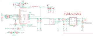
I have a design with a BQ25895 charger, a BQ27441-G1 fuel gauge and a 900mAh 3.7 Lipo battery. 

I am entering shipping mode and leaving the circuit on and routinely measure the battery voltage with a tool, and logging the results in a spreadsheet.

After 16 days the battery voltage has dropped from 4.02V to 3.67V, which indicates a power consumption of several mA.

However the BQ25895 specifies a leakage of 23uA maximum, and the BQ27441-G1 93uA if it's in Normal mode.

How can I explain this large power consumption? At this rate my battery will be fully depleted in about 4 weeks.

Please find a screenshot of that portion of the schematic. 

Thank you

  • Hi,

    The battery also connects to the fuel gauge. Please only connect the battery to the BAT pin of the BQ25895 and try the shipping mode again.

    Thanks,

    Ning.

  • Hello,

    Than you for the suggestion, however in my scenario it is not possible as I need to monitor the battery state of charge. 
    Is there a way to have some insight about the shipping mode leakage anyway? The fuel gauge is also a TI product.

    Are you able to check the schematic of the charger and fuel gauge and let me know if you find something off?

    Thank you

  • Testing a bit further, I realized that when I activate shipping mode ("Turn off Q4" in Battery Management Studio), the Vsys voltage does not reaches 0V, instead it stays around 1.2V. As a result, my 3.3V LDO which is connected to Vsys also has an output voltage of 1.2V. 
    I suspect that this is causing my entire circuit to draws a little bit of power instead of being complitely off.

    Please find attached a screenshot that shows VSYS on the scope.

    Any ideas?

    Thank you

  • Hi,

    We will get back to you on the next business day.

    Thanks,

    Ning.

  • Hello,

    Any news about this?

    Thank you

  • Hi,

    We are still and will get back to you today.

    Thanks,

    Ning.

  • Hello Coriolan,

    Can you give more details for your chargers register settings so we can test on our side?

    Are you able to confirm with an ammeter if the current loss is from the VSYS pin on the charger?

    Sincerely,

    Wyatt Keller

  • Hello

    Please find attached the current registers. They are very similar to the default registers.

    Regarding the current, my ammeter seems to indicate a current leak of about 900uA to 1mA, which is consistent with the battery discharge rate that I am seeing.

    Let me know if you need me to bring more information.

    Thank you

    Commnd	I2CSlv	Addr	Data	Comment (All Values in Hex)
    w	D4	00	52	#Input Current Limit, HIZ and ILIM pin
    w	D4	01	0A	#OTG Temperature thresholds, and Input Voltage DPM Offset
    w	D4	02	3D	#ADC controls, OTG Frequency, ICO, DCP, and Input Detection
    w	D4	03	3A	#Battery Load, WDT Reset periods, OTG and Charge Enable, and MINSYS setting
    w	D4	04	0E	#Fast Charge Current Limit settings and MTK Pump enable
    w	D4	05	13	#Pre-charge and Termination Current Limit settings
    w	D4	06	5E	#Charge Voltage Regulation Limit, Battery Low Voltage and Recharge threshold
    w	D4	07	8D	#Termination Current Enable, STAT pin, WDT, Safety Timer, and JEITA Charge Current
    w	D4	08	03	#IR Compensation and Thermal Regulation thresholds
    w	D4	09	44	#ICO, Extended Safety Timer, BATFET control, MTK Pump Voltage, and JEITA Charge Voltage
    w	D4	0A	93	#OTG Regulation Voltage and Current Limit settings
    w	D4	0B	3E	#Charger VBUS, Charging Mode, PG, USB Input, and System Voltage Regulation status
    w	D4	0C	00	#WDT, OTG/VBUS OVP, Thermal Shutdown, Safety Timer, and TS pin faults
    w	D4	0D	0F	#Input Voltage DPM settings
    w	D4	0E	5C	#Thermal Regulation Charge Status, and ADC Battery Voltage conversion
    w	D4	0F	5D	#ADC System Voltage conversion
    w	D4	10	60	#ADC TS pin voltage as percentage of REGN conversion
    w	D4	11	9A	#VBUS status, and ADC VBUS Voltage conversion
    w	D4	12	00	#ADC Charge Current conversion
    w	D4	13	12	#DPM status, and Input Current Limit setting
    w	D4	14	39	#Registers reset, Input Current Optimizer status, Device ID, and Temperature Profile
    

  • Hello Wyatt,

    Please find attached the settings in both "Standard Tab Separated Format" and "Test Output Format", so that you can load them directly on the Battery Management Studio GUI.

    Thank you

    Commnd	I2CSlv	Addr	Data	Comment (All Values in Hex)
    w	D4	00	52	#Input Current Limit, HIZ and ILIM pin
    w	D4	01	0A	#OTG Temperature thresholds, and Input Voltage DPM Offset
    w	D4	02	3D	#ADC controls, OTG Frequency, ICO, DCP, and Input Detection
    w	D4	03	3A	#Battery Load, WDT Reset periods, OTG and Charge Enable, and MINSYS setting
    w	D4	04	0E	#Fast Charge Current Limit settings and MTK Pump enable
    w	D4	05	12	#Pre-charge and Termination Current Limit settings
    w	D4	06	5E	#Charge Voltage Regulation Limit, Battery Low Voltage and Recharge threshold
    w	D4	07	8D	#Termination Current Enable, STAT pin, WDT, Safety Timer, and JEITA Charge Current
    w	D4	08	03	#IR Compensation and Thermal Regulation thresholds
    w	D4	09	44	#ICO, Extended Safety Timer, BATFET control, MTK Pump Voltage, and JEITA Charge Voltage
    w	D4	0A	93	#OTG Regulation Voltage and Current Limit settings
    w	D4	0B	67	#Charger VBUS, Charging Mode, PG, USB Input, and System Voltage Regulation status
    w	D4	0C	01	#WDT, OTG/VBUS OVP, Thermal Shutdown, Safety Timer, and TS pin faults
    w	D4	0D	0F	#Input Voltage DPM settings
    w	D4	0E	00	#Thermal Regulation Charge Status, and ADC Battery Voltage conversion
    w	D4	0F	00	#ADC System Voltage conversion
    w	D4	10	00	#ADC TS pin voltage as percentage of REGN conversion
    w	D4	11	99	#VBUS status, and ADC VBUS Voltage conversion
    w	D4	12	00	#ADC Charge Current conversion
    w	D4	13	12	#DPM status, and Input Current Limit setting
    w	D4	14	39	#Registers reset, Input Current Optimizer status, Device ID, and Temperature Profile
    

    * Created: Thu Apr 29 09:27:13 BST 2021
    *
    * Format: Register Name  tab Character,\t  Hexadecimal register value.
    * BQZ Container: Charger_1_00-bq25890_895.bqz
    *
    Input Current Limit, HIZ and ILIM pin	52
    OTG Temperature thresholds, and Input Voltage DPM Offset	0A
    ADC controls, OTG Frequency, ICO, DCP, and Input Detection	3D
    Battery Load, WDT Reset periods, OTG and Charge Enable, and MINSYS setting	3A
    Fast Charge Current Limit settings and MTK Pump enable	0E
    Pre-charge and Termination Current Limit settings	12
    Charge Voltage Regulation Limit, Battery Low Voltage and Recharge threshold	5E
    Termination Current Enable, STAT pin, WDT, Safety Timer, and JEITA Charge Current	8D
    IR Compensation and Thermal Regulation thresholds	03
    ICO, Extended Safety Timer, BATFET control, MTK Pump Voltage, and JEITA Charge Voltage	44
    OTG Regulation Voltage and Current Limit settings	93
    Charger VBUS, Charging Mode, PG, USB Input, and System Voltage Regulation status	67
    WDT, OTG/VBUS OVP, Thermal Shutdown, Safety Timer, and TS pin faults	01
    Input Voltage DPM settings	0F
    Thermal Regulation Charge Status, and ADC Battery Voltage conversion	00
    ADC System Voltage conversion	00
    ADC TS pin voltage as percentage of REGN conversion	00
    VBUS status, and ADC VBUS Voltage conversion	99
    ADC Charge Current conversion	00
    DPM status, and Input Current Limit setting	12
    Registers reset, Input Current Optimizer status, Device ID, and Temperature Profile	39

  • Hello Coriolan,

    What is your pull-up configuration? This may be causing the issue if the pull-ups are active when in shutdown mode, try disabling the pull up during shutdown if possible.

    I was able to replicate what you see with similar voltage, when the EV2400 is disconnected the voltage drops to 0V on VSYS.

    Sincerely,

    Wyatt Keller

  • Hello,

    Are you referring to the pull-ups for the signals STAT, PG, CE, INT, OTG?
    On my schematic I only pull up the INT pin, and it's pulled to the 3.3V line which comes from a LDO powered by Vsys. So if Vsys is turned off, the 3.3V should also be turned off, so that cannot be the root of the issue, am I correct?

    It would be impossible to pull up these signals to Vsys anyway because my microcontroller has a maximum input voltage of 3.3V, and Vsys can be up to 5V.


    Is there a register setting related to the pull-ups that I can change?


    Thanks

  • Hello,

    Are there any other ways to bypass the BATFET for your system? The most likely cause is there is some external pull-up applied on VSYS (the ones you mentioned or SDA and SCL)

    Sincerely,

    Wyatt Keller

  • Hello Wyatt,

    No there are no other way, we specifically chose the BQ25895 for its shipping mode feature. 

    I still don't see why the i2c pull-ups resistors would prevent Vsys from being at 0V?

    Is there another solution?

    Thanks

  • Hi,

    We are unable to duplicate your observation on the BQ25895 EVM. In order to verify your observation, please place the "issue" IC you have on a fresh working BQ25895 EVM and take the same test. If the behavior still exists, please let us know and we may do further research.

    Thanks,

    Ning.