This thread has been locked.

If you have a related question, please click the "Ask a related question" button in the top right corner. The newly created question will be automatically linked to this question.

BQ25171-Q1: application questions

Part Number: BQ25171-Q1
Other Parts Discussed in Thread: TPS63020, BQ25171EVM

Hello team. The question from customer. Thank you for support in advance.

We are going to use BQ25171 to charge a backup battery in our device.

There will be a situation, where main supply voltage is switched off, so Vin of BQ25171 is equal to 0V, and all of the system is supplied from Vbat.

So there are several questions on this:

1. While BQ25171_Vin = 0V, it results BQ25171 is supplied from Vout = Vbat = 2V4 – 4V5. Does BQ25171 contain a reverse current protection circuit? Is this mode allowable for BQ25171?We consider the situation when Vin = 0 may continue very long, till Vbat = 0.

2. What the amount of reverse current will flow into  BQ25171, when Vout = 4V5?

3. Does BQ25171 contain a reverse battery protection?

4. To get the temperature value of battery, we want to measure the voltage on BQ25171_TS pin by ADC of external CPU. Can we connect TS pin directly to CPU_ADC input?What is the maximum voltage range of TS pin in the range of temp -40...+85C? 

  • Hello Slava,

    1. The bq25171 will prevent current flow from OUT to IN.
    2. OUT = 4.5V will be very close to these values ( < 1uA) 
    3. The asb minimum rating on the OUT pin is -0.3V, connecting battery in reverse will likely damage the IC.
    4. TS voltage is clamped at 2.6V when floating. You can connect TS pin to MCU as long as it is a high impedance input so it doesn't interfere with the readings.

    Best regards,

    Nick

  • Hello Nick,

    Thank you very much for your answer! This question was for our company. I have some additional questions:

    Our design contains TPS63020 buck-boost converter for power supply of our CPU (Vin = 2-4.5V / Vout=3V3). Vin of TPS63020 connect to rechargeable battery, rechargeable battery connects to OUT of BQ25171. As I understand from BQ25171 datasheet, CE pin may be control from our CPU (HOST). CPU output pin level is 3V3. A situation may arise, when BQ25171_Vin = 0V, BQ25171_OUT = 2V and BQ25171_CE = 3V3 (CE pin controls from out CPU), i.e. BQ25171_CE (3V3) > BQ25171_Vin (0V) and BQ25171_CE (3V3) > BQ25171_OUT (2V).


    • Is the situation acceptable, when BQ25171_CE (3V3) > BQ25171_Vin (0V) and BQ52171_CE (3V3) > BQ52171_OUT (2V) very long? May be damage of BQ52171 in this situation? The situation when BQ25171_Vin = 0 / BQ25171_OUT = 2V / BQ25171_CE = 3V3 may continue very long.
    • As I understand from BQ25171 datasheet there is Vin_uvloz But unfortunately, I cannot find level of Vin_uvloz in datasheet. What is the level of Vin_uvloz (mV)?


    Best regards,

    Ruslan,

    Developer engineer, Fort-Telecom, Perm, Russia.

  • Hi Ruslan,

    1. As long as you are staying under the max rating on the /CE pin you are OK ( 5.5V) . The /CE pin is connected to an input of comparator.

    Best regards,

    Nick

  • Hello Nick,

    Thank you very much for your answer! I have some additional questions.

    We have to use 3-cells V500HT (Varta) Ni-MH rechargeable battery in our design. As I understand from V500HT datasheet maximum charging voltage for V500HT cell is 1V4 at +60C, 1V5 at +25C and 1V6 at -10C. Charge curves with 0.1CA (50 mA) at various temperatures file is attached to this post. Therefore, for 3-cells V500HT Ni-MH rechargeable battery maximum charging voltage is 4.2V at +60C, 4.5V at +25C and 4.8V at -10C. Other models of 3-cells Ni-MH rechargeable battery has the same maximum charging voltage characteristics. We have charge out battery at -10C to +60 C temperature.

    As I understand from BQ25171 datasheet (Table 7-2. VSET Pin Resistor Value Table) I should set 18kΩ VSET resistor (4.20V/3-cell+intermittent charge). CHM_TMR pin resistor is 24kΩ (NiMH/8hr). ISET resistor set for 70mA charging current. We tested charge battery at +25C temperature, therefore, for 3-cells V500HT Ni-MH rechargeable battery maximum charging voltage is 4.5V. Our battery voltage has reached 4.2V and charge was completed trough 4 hour instead 8 hour (STAT[1..2] = b11). Then we discharge this battery with the help our electronic load, battery capacity is 300mAh instead nominal capacity 500mAh. Therefore, our battery was not fully charged! It is very badly…

    As I understand from Charge curves with 0.1CA (50 mA) at various temperatures file of our battery I should set VSET resistor to 4.8V, because maximum charging voltage is at -10C. We have use intermittent charge too. But unfortunately, I cannot find 4.8V level (3-cells/Ni-MH+intermittent charge) at Table 7-2 (VSET Pin Resistor Value Table).

    • What is VSET resistor I should set at BQ25171_VSET pin for our battery?
    • How to charge our battery fully (to 500mAh) with the help BQ25171? What is the value VSET/ISET/CHM_TMR resistors I should set to BQ25171 pins?

    Best regards,

    Ruslan,

    Developer engineer, Fort-Telecom, Perm, Russia.

    V500HT Charge curves with 0.1CA (50 mA) at various temperatures.pdf

  • Hi Ruslan,

    Can you attach the schematic for review? With your configuration the device should stop charging after the 8 hour timer expires. If it is stopping at 4.2V you may want to verify you have the correct resistances on VSET and CHM_TMR.

    Thanks,

    Nick

  • Hello Nick,

    Thank you very much for your answer! I have some additional questions.

    • As I understand from your answer: «As long as you are staying under the max rating on the /CE pin you are OK ( 5.5V) . The /CE pin is connected to an input of comparator». I have additional question. As I understand internal input comparator on CE pin has 2V internal power supply, when BQ25171_Vin = 0 / BQ25171_OUT = 2V. Therefore, if BQ25171_CE = 3V3, then BQ25171_CE (3V3) > internal power supply of this comparator. I think cannot be situation with over rail-to-rail voltage for inputs of this internal comparator, when BQ25171_CE=3V3.

      Is there internal divider on BQ25171_CE pin before internal input comparator? Then internal power supply of this comparator will be more middle point of internal divider on BQ25171_CE pin and this comparator will be at rail-to rail mode. Is it correctly?


    • If internal divider on BQ25171_CE pin before internal input comparator is absent, then I don’t understand situation with over rail-to-rail voltage for inputs of this internal comparator. I'm afraid that BQ25171chip will damaging.

      Do you confirm that as long as you are staying under the max rating on the /CE pin you are OK ( 5.5V)? Сan you explain the situation?


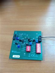
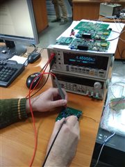
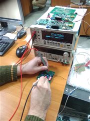
    • We use your BQ25171EVM board for testing our Ni-MH rechargeable battery. Schematic of BQ25171EVM is on the website TI. We have set the following settings for BQ25171EVM:
      - JP1 set between pin 1 and pin 2
      - JP2 (CE) set between pin 1 and pin 2 (CE is ON)
      - JP3 (ISET) set between pin 1 and pin 2 (ADJ mode) and R21 + R22 = 4.44 k Ohm (about 70mA)
      - JP4 (STAT1) set between pin 1 and pin 2 (STAT1 is ON)
      - JP5 (STAT1) set between pin 1 and pin 2 (STAT2 is ON)
      - JP6 (TS-ADJ) is absent. TS pin connect to our NTC 10K resistor, which is inside our battery trough J2.1 pin.
      - JP7 (CHM_TMR) is absent. S2 in ON between pin 4 and pin 5 (R14=0R), rest S2 switches is OFF. R10 = 24 kΩ.
      - JP8 (VSET_ADJ) is ON (R9 = 0R), S1 in ON between pin 4 and pin 13 (R4 = 18 kΩ), rest S2 switches is OFF.

      We tested all resistors with the help DMM4040 Tektronix multimeter: CHM_TMR (between TP6 and GND) = 24 kΩ, VSET (between TP9 and GND) = 18 kΩ, ISET (between TP6 and GND) = 4.4 kΩ. Picture files is attached to this post.

    • What is VSET resistor I should set at BQ25171_VSET pin for our battery?
    • How to charge our battery fully (to 500mAh) with the help BQ25171? What is the value VSET/ISET/CHM_TMR resistors I should set to BQ25171 pins?

     Best regards,

    Ruslan

  • Hello Ruslan,

    1. There is no damage to the device if left with /CE at 3.3V and OUT at 2V. The max rating on /CE is 5.5V, not dependent on the OUT voltage.
    2. For 3 cell NiMH with intermittent charge and 8 hour timer you have configured it correctly,  VSET with a 18 kΩ and CHM_TMR with 24 kΩ. Was there any faults present on STAT 1/2 that would have stopped the charge early?

    Best regards,

    Nick

  • Nick, let's put this discussion on hold.

    Ruslan will check samples of series device BQ25171QWDRCRQ1 (not P variant provided before|).

  • OK, also note that once a value has been detected, it is latched in and the pin is not continuously monitored during operation. A change in this VSET or CHM_TMR value will not be acknowledged by the IC until the input supply or CE pin is toggled.

    Thanks,

    Nick