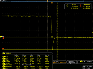
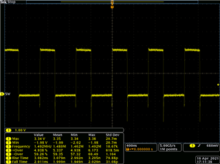
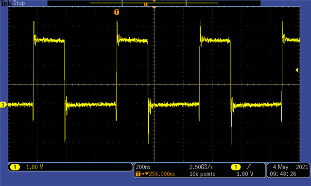
I observed some ringing at the SW node, which causes it to have negative spikes at every switching cycle. I measured close to -2V for about 5ns. In the datasheet the minimum voltage specified is -0.3V for SW pin. Is this spike acceptable?

-
Ask a related question
What is a related question?A related question is a question created from another question. When the related question is created, it will be automatically linked to the original question.