This thread has been locked.

If you have a related question, please click the "Ask a related question" button in the top right corner. The newly created question will be automatically linked to this question.

UCC2818: free running frequency variation

Part Number: UCC2818
Other Parts Discussed in Thread: UCC3818, UC3854

Hi all,

We are using the UCC2818 with the synchronisation circuit refered in application note "SLUA245 - July 2000".

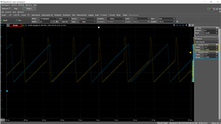
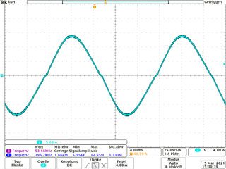
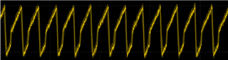
Like described in application note "SLUA296A - October 2003 -- Revised April 2010" we can observe the negative effects on the current (left image).

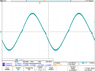
Without synchronisation (and a smaller CT to maintain 145kHz switching frequency) those effects are non present anymore (right image). 


However in free running mode the frequency tolerance from the datasheet is very high with +/-20%.

Which parameters have the most effect on this variation?

Assuming RT and CT have 0% tolerance what would be:

-the variation between different devices?

-the drift from the initial frequency over a lifetime of 10 years?

Best regards,

Michael

  • Hello,

    I am not familiar with the synchronization circuit presented in slua296a.  I have used the sync circuit presented in slua245.  The following link will bring you to the application note.  I would give this a try to see if your operation improves. 

    https://www.ti.com/lit/an/slua245/slua245.pdf

    Synchronizing the frequency should not create cross over distortion in your low frequency line current.  The current loop should not be responding to the high frequency current and should cross over at a 10th of the switching frequency.

    I would suggest studying the oscillator frequency synchronized and unsynchronized to make sure it looks and behaves the way you expect it too.  The application note shows what the oscillator waveforms should look like. 

    Generally the PFC stage is setup to operate at a slower switching than you synchronize too.  If your design without synchronization is at 100 kHz, you can synchronize it to a faster switching frequency.  For example 120 kHz would be a good target.   If you are trying to sync to a similar frequency or slower frequency, you will not be able to get proper synchronization.  This could lead to circuit misbehavior and EMI issues.  This is covered in detail in application note slua245.

    What generally causes crossover distortion.

    1. Current amplifier offset and not being able to achieve 100% duty cycle at crossover. 

    2. Voltage loop and current loop is not commentated correctly.

    Recommendations/options:

    1. Try alternative synchronization scheme slua245

    2. Double check sync circuit and make sure the design is synchronized to a faster switching frequency.

    3. Make sure the sync circuit is not adding offset to the current amplifier or grounding.

    4. Double check the voltage loop and current loop small signal stability.

    Regards,

  • Hello,

    thank you for the fast response. 

    At the pins from the IC there are no differences measurable. 

    The picture shows the synchronised waveform and the unsyncronised one (two different modules)

    The free running frequency is set to 116kHz and it gets synchronised to 145kHz. With the synchronisation the gate is driven at a frequency of 145kHz.

    For the module with free run we have also tried a smaller CT to have free running 145kHz but no distortion on the mains current were visible. 

    1&2) It does work properly in free running mode so the circuit should be ok?

    1) There is already a layout/ many modules manufactured. It is a follow up question from this topic -> https://e2e.ti.com/support/power-management/f/power-management-forum/993438/ucc2818-synchronization-oscillator-circuit-documentation/3669392#3669392

    2) For this specific module it is 112kHz free running and 145kHz synched. 

    3) The sync circuit is a few cm away from the UCC and directly connected to the ground plane. No current e.g. recharging of the bootstrap is flowing near or across the UCC

    4) As it is working in free running mode at frequencies below and above 145kHz this should also be fine?

    slua245 mentions 3 benefits compared to slua296a.

    1. Synchronization of converters where the timing capacitor is unavailable and there is no synchronization pin available.

    2. Uniform ramp amplitude from unit to unit therefore stable voltage gain and current compensation.

    3. No distortion of the ramp which allows for maximum duty cycle limiting.

    Does 2) implies the gain of the internal amplifiers gets distorted if you use this synchronisation circuit?

    Does 3) implies the duty cycle gets limited proportional to f_free/f_sync?

    Best regards,

    Michael 

  • Hello,

    Could you study the current amplifier output, multiplier output, CAOUT and current sense signal for synchronized and unsynchronized?

    This may tell you what is going on and why there is increased cross over distortion.  You may even want to study your inductor current as well.

    At higher frequencies your inductor current could be going discontinues that could lead to crossover distortion.  The synchronization should not by itself should not generate more crossover distortion. 

    You are correct that you can not obtain the same maximum duty cycle with the sync circuit of slua245.  The CT discharge time is dead time.  And could lead to cross over distortion.  You had mentioned that set the frequency to 145 kHz and there is no distortion.  Maybe it is contributing to cross over distortion.  It may be worth giving the circuit presented slua296a a try.


    You do have another option. The oscillator timing is setup with a Rt and Ct.  You could use a larger Rt and smaller CT to get the same frequency.  This will reduce the dead time and may remove the crossover distortion as well.

    Regards,

  • Hello,

    the dutycycle got limited from 92% unsynchronised to 85% synchronised. Therefore the PFC was not capable of boosting voltages <60V and the current controller got saturated. 

    However reducing CT from 470pF down to 100pF only brought minor improvements. To me it seems the discharge time is limited by the controller itself. Additionally a CT of 100pF would result in a bootstrap capacitor >24pF. To have some tolerance 30pF were tested. It works fine for 85VAC-230VAC. Above 230VAC (up to 265VAC) the mains current gets distorted again. (It looks fine while free running at 145kHz).

    Using a bigger bootstrap capacitor leads again to a longer discharge time and therefore more crossover distortion.

    130V mains, 230V mains, 265V mains

  • Hello,

    The discharge current to CT is fixed and while it is being discharged the gate drive is off.  So you are correct that it will lead to limiting the duty cycle.  The design should still meet EN61000-3-2 harmonic requirements and most agency requirements even with a flat spot in the input current.

    I am not sure how adjusting the CT and RT leads to bigger boot strap capacitor.  Adjusting the RT and CT should be a viable option for reducing the dead time. 

    There is another option you could use a UCC2854B with trailing edge modulation and synchronize the down stream converter with the UCC2854B's gate drive.  This technique will have no l imitation on UCC2854B's maximum duty cycle. 

    Regards, 

  • Hello,

    the flat spot would not be a problem but the resonant behaviour at 265VAC mains is. 

    The charge on the bootstrap must be enough to charge CT above its threshold voltage. Otherwise the synchonisation would look like this:

    A change in the shematic or even the controller is not a real option at this stage of our project. 

  • Hello,

    That is a strange behavior.  I would not think changing the RT and CT ration would do that.  The RT sets the charge current.

    I do not know of any other way to synchronize the UCC3818 that is presented in the application note.  It does limit the duty cycle and will lead to some flat spots at crossover.

    In regards to resonant behavior on the mains I can see a spike after the flat spot.  Is that the issue you are talking about?  If so try adjusting your EMI input filter to get rid of it.

    Regards,

  • Hello,

    the spike after the flat spot is caused by the current controller which gets saturated at crossover. 

    At higher AC input voltages the distortion around crossover gets bigger until at 265VAC the signal is completly distorted. Unsynchronised at 145kHz no problems can be observed. These distortions only appear in combination when synchronising the controller. 

    How big is the variation in frequency in the free running mode?

  • Hello,

    The CS signal is smaller at high line and is contributing to the cross over distortion.  This can be reduced by increasing the CS signal.

    The reduced duty cycle caused by the sync circuit also causes the increased flat spot at cross over.  Please note this should still meet EN61000-3-2 harmonic current requirements.

    I reviewed the data sheet and the frequency variation is specified as +/- 20%.

    Regards,

  • How can the CS signal be increased? Does this implie to correctly synchroniese the chip we would have to change the bootstrap capacitor accordingly to the line voltage?

    Are those +-20% variation over different devices or line, temp, etc.?

  • Hello,

    Increasing the resistance of the current sense resistor will increase the current sense signal.

    The data sheet specifies the teampature range that that the device parameters are guaranteed  too.

    How is the boot strap capacitor related to sync the chip?  This generally the VDD or VCC capacitor and sized with charge control law I = C*dv/dt

  • Hello,

    Without the synchronisation circuit from "SLUA245 - July 2000" there are no big crossover distortions. With the synchronisation the behaviour of the chip changes dramatically and does not meet the requirements (see my post from may 7th 10:06AM). 

    Unsynchronised would be viabel but with +-20% tolerance in frequency it is nearly impossible to make correct filter design and get emc correct. 

  • Hello,

    The cross over distortion create is caused by the limit duty cycle caused by the sync circuit, which you verified.  When the converter is unsynchronized there is no limitation on the duty cycle with lower cross over distortion.  The dead time of the gate drive takes place during the CT discharge.  To try to reduce this it was suggest to lower the CT.  However, this did not give you the performance you had before. 

    This synchronization technique  does meet EN61000-3/-2 harmonic requirements even with  the increased flat spot.  The synchronization technique was developed back in 2000.  I was not aware that this sync circuit limited the duty cycle but it makes sense.

    You were able to get rid of the distortion by setting the oscillator to a faster frequency.  By adjust CT to have the free running frequency at 145 kHz.  Could you try using the same CT and adjust RT for the lower frequency to  see if the cross over distortion is reduced.

    If reducing the CT does not give you the desire behavior when synchronizing there are other option is to select a PFC controller like the UC3854 that using trailing edge modulation and synchronize the  down stream converter from it.  In this fashion the synchronization will not affect the maximum duty cycle of the PFC controller. 

    I reviewed SLUA296A which uses a phase lock loop to sync the PFC.  It adjust the oscillator charge current and the oscillator ramp does not seem to be affected by the synchronization.  You might want to give this sync circuit a try as well to see if you can get better performance.

    Regards, 

  • Hello,

    the flat spots at crossover are not my problem but the oscillation the whole current is. This is already with a reduced CT. It does only occur when synchronising. While free running at 120kHz and 145kHz there are no oscillations.

    The chip/synchronisation circuit is fixed and cannot be changed unfortunatelly. 

  • Hello,

    The following is the waveform you reported and issue on.  Has this changed?  This is caused by the limited duty cycle of the sync circuit you verified.

    Regards,

  • It has changed 4 days ago in my post from May 7th 10:06AM

  • Hello,

    Could you tell me what the THD and PF is for the waveform in question?

    I did review your last waveform below and can see high frequency ringing on it.  I would not think this would be due to the sync circuit.

    Is this the waveform in question?

    Regards,

  • Even if the THD and powefactor meet the requirements there is something wrong with this waveform that needs to be solved.

    Unsynced at 145kHz: Proper sine wave with little to no distortion at crossover

     Unsynced at 120kHz synced up to 145kHz: The waveform from above with a lot of ringing. 

  • Hello,

    You need to figure out why the low frequency ringing is where it is.  Once you do that you may be able to remove it.

    I would start by looking at the Multiplier output, current amplifier output, voltage amplifier output  to make sure there is no high frequency noise on it and it looks like you expect it too.  If it does not try to clean this up.  If not it is something else.

    If the multiplier, voltage amplifier and current amplifier look O.K.  The I would study the switch node, inductor current and current sense signal to make sure they behave as expected.  This may help you figure out were this noise is coming from.

    I had one last thought.  When you had the CT set at 145 kHz and not synchronized did you  have that high frequency ring disturbance?

    >If not the sync signal may be injecting noise into the ground or systems creating the disturbance.  I do think this would be everywhere in the line cycle if this was the case.

    >The ring you have presently does look sinusoidal and not critical damped.  If could be the current loop or voltage loop does not have enough phase margin.

    Regards,