This thread has been locked.

If you have a related question, please click the "Ask a related question" button in the top right corner. The newly created question will be automatically linked to this question.

TPS63010: Leakage current Issue

Part Number: TPS63010

Hi, 

We are using TPS63010YFFR in our enterpise mobile phone design. We are observing an issue with respect to leakage current in TPS63010 in some of the boards.

The TPS schematics in our design is as below:

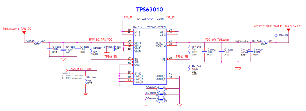
  • Input to TPS is 4V(RAW_DC)
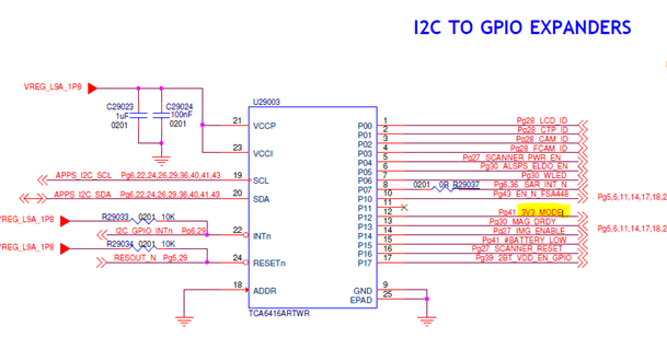
  • PSn pin(3V3_Mode) is driven by an I2C based GPIO expander

The setup to measure leakage current is as below:

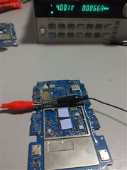
  • An input of 4V is fed to the board without powering ON the board.
  • A leakage current of around 6mA is observed in some of the boards, roughly in 4 out of 15 boards that we have.
  • If the TPS63010 is disabled by pulling the enable pin low, leakage current is not observed thus proving that the leakage is indeed caused by TPS63010.
  • This leakage current is observed when the board is first powered up.
  • If the power supply is removed and fed back immediately, the leakage current is not observed.
  • If the power supply is removed and fed back once the output capacitor is completely discharged(takes around 10-15 seconds), the leakage current is again observed.
  • The output voltage in both high and normal leakage current cases is about 3.25V.

We have captured the waveforms(LX1, LX2, VOUT ripple) with and without the leakage current. Please find the doc with images attached.

TPS63010 Waveforms.docx

We tried the following experiments:

  • Isolated the PSn pin from the GPIO Expander and pulled it down to ground through 0 Ohm(R41050), the leakage current(~6.2mA) was still observed.
  • Isolated the load connected to TPS63010 by removing output series resistor (R41046), the leakage current still remained.
  • We swapped the TPS63010 chip between a good and a bad board and the issue followed the IC, i.e, Good board started showing leakage current and the bad board was normal. We performed this experiment twice with different set of boards and the observations were same.

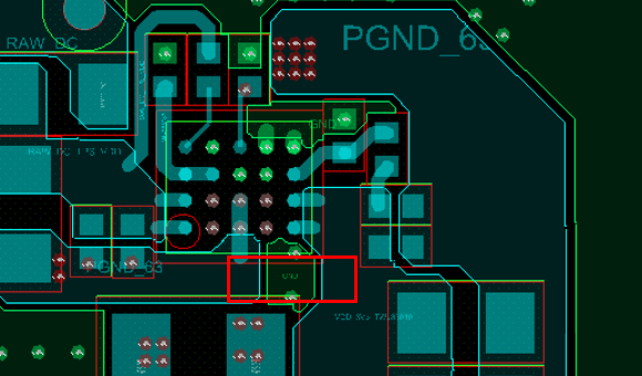
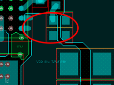
The layout section of the TPS63010 is attached for your review.

TPS63010_LAYOUT.pptx

Since this issue is not reproducable in all the boards, we are finding it hard to figure out the root cause for this leakage current.

Kindly review the design and our observations. Please do let us know if you need any inputs from us.

Your timely suggestions and inputs would be invaluable for us as we are approaching the Mass production stage for this product.

Thanks,

Naveen

  • Hi Naveen,

    In the attached waveforms, the bad boards seem to work in force PWM mode while good boards work in PSM mode. Are you sure all board ICs' PS pin signals are the same?  If IC works in force PWM mode, the input current will be higher and efficiency is low. The leakage current is 5.8mA in force PWM while it is 0.053mA in PSM during bench EVM test. 

    I think enable all board ICs' PS pin to work in PSM mode can decrease leakage current when the load is small or even open load.

    Best Regards,

    Eric Yue

  • HI Eric ,thanks for your answer, How to set this IC to PSM mode?

    Also add a phenomenon of this issue,

    when we reduce the input voltage to below 3.6V slowly,  this issue is disappear.

    If we insert a low voltage battery(low than 3.6V) at first, also no this issue.

  • Could you help to left your phone number? i suppose you are in china. thanks a lot.

  • Hi Eric, 

    We put 1 nF capacitor across the feedback resistor R41048 and the issue seems to have resolved. We tried this in three bad boards. Please let us know your thoughts.

    Thanks,

    Naveen

  • Hi Brain,

    PSM mode can be enabled by set PS pin to low which can be specifically found in 8.4.4 of datasheet. The PS input supports standard logic threshold voltages. Please make sure PS is set to low, you can test PS pin voltage and measure LX1, LX2 waveforms to confirm. In the provided waveforms of LX1 and LX2, the bad board's IC is still switching.

    Sorry, my phone number is not convenient to provide here because E2E website is open. I will keep track of the problem's progress until it is resolved

    Best Regards,

    Eric Yue

  • Hi Brain,

    please try place one ceramic capacitor in the rectangle area.  not sure if this is caused by the layout. also what is SG4100?

  • Hi Jasper/Eric

    We found the we can solve this issue by change the 1M resistor and 180K resistor to 500K and 90K, But we don't know if there will be other issue. Could TI give some suggestion about these two resistors base on the IC design?

  • Hi Brain,

    Typically, there is no need to parallel a capacitor across the feedback resistor because IC is designed to have good loop stability and enough margin. For feedback resistors, recommended value for R41049 should be lower than 500 kΩ in order to set current through the resistive divider is about 100 times greater than the current into the FB pin. R41048 is depend on the needed output voltage.

    It now appears the problem can be resolved by adjusting feedback section to change loop function. Not sure whether PCB layout causes this issue, the layout seems have several problems:

    1. What is SG4100? IC's AGND and PGND seems not connected to one node close to ground pins of IC. Power ground and control ground should be connected to different nodes and connect together to minimize the effects of ground noise. This may cause IC cannot enter PSM mode normally.

    2.The power path is long and output capacitors are far from IC. Typically, use wide and short traces for main current path and power ground tracks. The input capacity, output capacity must be placed close to IC.

    3.Several pins of IC e.g. Vin, Vout, VSEL should be connected to power or GND path by place polygons instead of several mils tracks to reduce the length of current loop.

    Additionally, in this situation, IC should work in PSM mode. You can measure waveforms of LX1, LX2, Vout ripple (DC coupling, 3.3V offset) to confirm whether IC enter PSM successfully.

    Best Regards,

    Eric Yue

  • Hi Eric,

    Yes, you are right, from the layout, it seems the SG41000/SG41001/SG41002 are useless to schematic.

    The layout placement and trace do need some improvement. Thanks for you suggestion.

    HI  Naveen

    Suggest change the layout placement as Eric suggest in other SKU(not in MVT SKU), then we test with now PCBA. thanks.

  • Hi  Eric

    Because this SKU is in PVT, so can't change the layout, Because we can solve this issue by changing the two FB resistors, could you give the suggestion how to chose the two resistors value?

    Can we use the resistors 560K and 100K? will there be any other issue if we use 560K and 100K value?

  • Hi Brain,

    The two resistors are programming output voltage and are related to loop stability. Typically, current through the resistive divider should be about 100 times greater than the current into the FB pin, so the recommended value for R41049 should be lower than 500 kΩ, in order to set the divider current at 1 μA or higher. The recommended value for this resistor is in the range of 200 kΩ from datasheet. More detailed introduction can be found at 9.2.2.1 from datasheet.

    It seems changing FB resistors maybe can reduce the impact of board noise, which may caused by layout. You can change R41049 to 100k because it is lower than 500k. Loop stability will not be affected very much, while efficiency will decrease slightly.

    Moreover, you can try to optimize the layout problems on existing board. The first two layout issues should be the main issues. IC's AGND and PGND can be connected to one node close to IC by flying wire or welding. One output ceramic capacitor can be added close across IC Vout and GND pins just like Jasper suggested.

    Best Regards,

    Eric Yue