This thread has been locked.

If you have a related question, please click the "Ask a related question" button in the top right corner. The newly created question will be automatically linked to this question.

LMG5200: LMG5200 random broken ICs

Part Number: LMG5200

Hello,

as we want to finish our Prototypes we occured that sometime LMG5200 seem to blow up for no reason during On/off test.

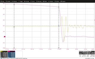
I followed the layout recomendations quite good so I started measuring on SW > PGND and found a -7V peak every time SW goes of. That's quite a problem because this pin is only specified for -5V. I'm now wondering if my Inductor might be to big. I used 33uH. Or what other reason could it be?

Is there any application note for GaN half bridge inductor calculation?

Technical details:

Vin: 60V, Vout: 50V, Iout: 5A, Cout: 800uF for low ripple

Thanks in advance

Marcel

  • Hello Marcel,

    Thank you for the summary - I don't think it is the inductor sizing that would cause the IC damage.  Are you able to take a scope picture of your input during turn on / turn off?  I noticed on your schematic you only have ceramic capacitors and if you are testing on the bench with a long cable without bulk capacitance you are likely to get an inductive kick and overshoot the 100V rating of the device. 

    If that is not the problem or does not help, please also take a scope shot of the SW, HI and LO pins to observe if any shoot through is occurring.  If HI and LO overlap there will be high dissipation in the device that could cause the problem.

    Regards,

    Steve

  • Hi Steve,

    thanks for your answer. My bad, I forgot the other schematic page here. Of course there are two 390uF Elkos additionally. I also already checked if there is any shoot through. It isn't. we have a 20ns deadtime and in the scope you can see these very nice.

    Also this is already a fully functional board. there are no cables at all. I will add some pictures.

     Pic from the board

    Yellow line is Pin 1 to 9. (Vin to PGND)

    Vin is 57V, so a 57V offset is on the channel. and it's 1V/div

    Pink line is Pin 8 to 9. (SW to PGND) first marker you could see beginning of the deadtime (-26,1ns). Second marker the low FET switches on. And then the voltage goes down to nearly -10V (-5V is max rating in the datasheet)

    As you can see in the other pic I nearly copied the eval board. No unneeded distance, everthing close to LMG. There are also additional ceramics on the  bottom side for Vin.

    Update:

    I tried to avoid this spike by:

    using a diode from 8 to 9, to cut the reverse voltage. LMG5200 immediatly died

    using a snubber RC from 8 to 9, to lower the spikes. LMG5200 immediatly died

    LMG5200 seems to be very sensitive at this point?

    Regards

    Marcel

  • Marcel,

    Thank you for the additional details - they definitely addressed my initial comments.  Regarding the -10V ring - just as a general recommendation you should always make sure the voltage stays within the datasheet specifications and tuning the layout to minimize the ring is a good idea.  However being said, from your description it does sound like something else is going on with the board that is causing the destructive failure.  Especially because you already tried putting a diode across the low side FET that should have clamped the voltage and prevented the internal driver from latching up.  In general you should expect a ~3V drop across the GaN FET in reverse conduction, and the part has been designed to handle that condition.

    The part has been in production going on five years and has proven to be pretty robust, so there is not a non-obvious sensitivity that I can point you towards.  Do you have any images of the damage, or do you observe any high case temperatures immediately before the event?  The waveform you shared looks to be steady state and at a very short time scale - do you have any other waveforms both at steady state and during the strart up / shutdown sequence that you can share to help provide a broader context?

  • Hi Steve,

    there is no visual damage at all, also no real heat up. Just the to FETs are cutted short. We also made Longtime tests with and without load, with no problems. These problems just accoured when we startet "on/off" tests.

    I added all 6 layers from the layout, perhaps you can see something I missed. I will add some scope pictures later this day.

    LMG5200_Layout.zip

    1% duty cycle, no load48% duty cycle, no load

    As you can see our first pulse (start up) is quite a shock for the board (-10V peak). Running up PWM it becomes better by every pulse. at 50% we have -5V. But normaly we work on 90%, so it becomes bad again.

    Is there a option to influence slewrate by gate resitors? as you can see I have provided some.But I guess not.

    It could be we have a ground floating problem here.

    Thanks for the additional information so far, I will keep up with my investigation.

  • Hi, Marcel,

    Sorry for the delay. What is the latest with your issue?

    Best regards,

    Don

  • Hey Don, it may be that we have a disturbance on the HI and LO input signals, which ends up in a shoot through sometimes. One of your german colleagues sent us the LMG5200 eval board, so we could evaluate if the error is reproducible. After everything Steve told me it seems not realistic that the IC itself is the problem.

    Anyway, if you have further suggestions you are welcome Slight smile

    Best regards

    Marcel

  • Hi, Marcel,

    Yes, evaluating the EVM is a great debug tool. Let us know how it works out.