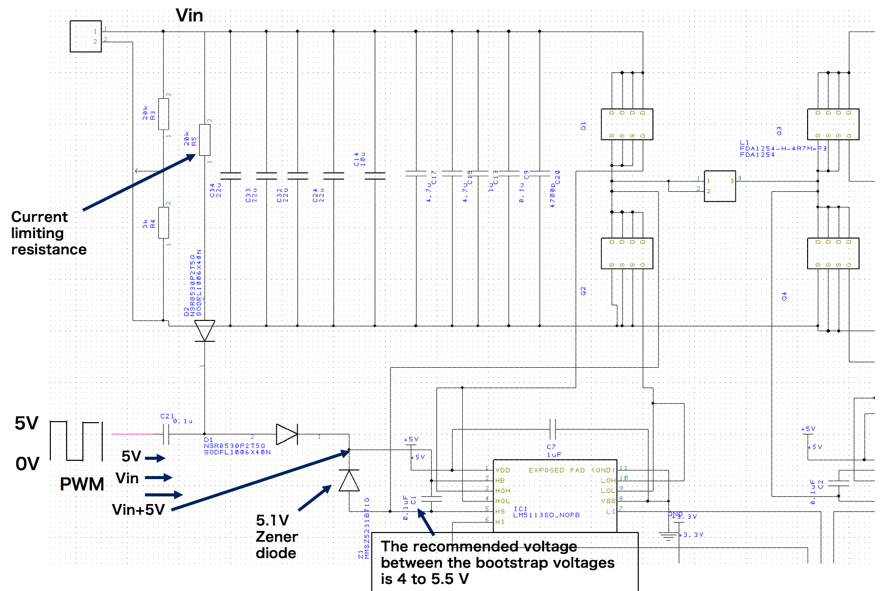
This thread has been locked.
If you have a related question, please click the "Ask a related question" button in the top right corner. The newly created question will be automatically linked to this question.
I’m sorry for my poor English.
I am studying H-bridge Buck-Boost converter. H-bridge Buck-Boost converter has 3 modes; Buck mode, Buck-Boost mode, Boost mode. When in Boost mode, SW1=ON, SW2=OFF, SW3=SW4=ON or OFF.So, SW1 needs Duty100%.
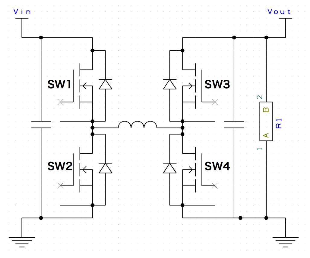
But when the drive method of the high side mosfet is set to the bootstrap method, the power of the bootstrap capacitor is exhausted, and 100% duty is not achieved. I used ucc27201(gate driver). When trying to operate at 100% duty, Undervoltage Lockout (UVLO) worked and Sometimes the duty ratio was not 100%. Undervoltage Lockout makes boost mode work. But Undervoltage Lockout causes noise.
How can I achieve 100% duty? Is Undervoltage Lockout the best method? Or Should I add another circuit like a charge pump circuit?
my application is Vin, Vout=3~20V, Iin, Iout=0~3A. I am using digital control with MCU.I will use lm 5113(Gate Driver) in the future. I am not considering pmos for the convenience of my application.
Thank you very much. I want to listen to other people's opinions, so I will continue to ask this questions.
Hi JapaneseStudent,
Sounds good, I can ask the rest of my team this question and see if they come up with anything different. I will also keep this thread open for you to seek more opinions.
Thanks
Hello Japanese Student,
I am an applications engineer at Texas Instruments and will work to answer your questions. I reviewed a previous post by Jeff, who provided good advice on using the UCC27201 driver with 100% duty cycle on the high side drive.
As was mentioned, to provide DC drive for the high side, a small floating bias supply needs to be provided for the HB-HS high side driver bias to sustain constant on time. TI has a device well suited for the bias which is the SN6505. You may need to add some components to make sure the HB-HS bias stays within its operating range such as some load resistance, or limiting zener diode.
Dear user3487469, Richard
I'm sorry for my late reply, and thank you for your reply. The LM 5175 is a great suggestion. But for my convenience, I can not use the LM 5175. I have to use a MCU.
I am very interested in how the LM 5175 achieves Duty 100%. But maybe it's a trade secret. But if there are little hints, I want it. For example, whether 100% duty is realized with a transformer or whether it is realized by charge charge.
Hello Japanese Student,
Thank you for the continued interest in the UCC27201, for my suggestion on 100% high side duty cycle we will recommend the high side floating dedicated bias supply. For the LM5175, I will refer you to another product line who is more familiar with this part.
Regards,
Richard Herring
Everyone
I thought about a circuit to achieve 100% duty as below. Do the following circuits operate correctly?
I made Vin + 5V by adding a charge pump circuit. LM5113's recommended voltage between the bootstrap voltages is 4 to 5.5 V. So, I clamped with a 5.1 Zener diode. I am concerned about the transient situation.
In creating this circuit I referred to “Providing Continuous Gate Drive Using a Charge Pump, TI"
Thanks,
Hello Japanese Student,
I am an application engineer with TI, and have responded to previous posts about this application.
In principal it looks like the charge pump should work. But you may want to confirm the effects of the diode drops from VIN and to HB. It looks like when PWM is 0 you will have 99.3V on the cathode of D2/anode of D1. When PWM is 5V you will have 104.2V at that same node to charge HB. It may take a slightly higher PWM signal.
For the transient conditions there may need to be some limiting resistance either in the PWM source waveform or in series with D1.
Regards,
Richard Herring