This thread has been locked.
If you have a related question, please click the "Ask a related question" button in the top right corner. The newly created question will be automatically linked to this question.
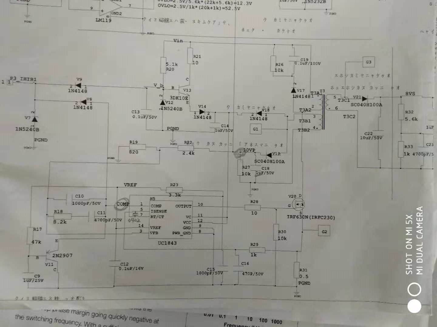
I made a flyback circuit based on UC3843.
When the input voltage reaches 40V, the duty cycle is unstable, and the phenomenon is suddenly large and small, which varies between 0.2 and 0.25.
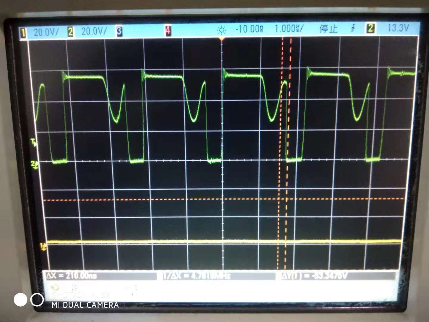
As shown in the figure below, the MOS tube drain source Voltage waveform.
我测试了此时的伯德图,如下图:
At this point, the phase margin is 51 degrees and the gain margin is -33dB. The loop parameters are still quite good.
I don't know what caused this? The loop is stable, but the actual drive wave D is unstable.
Hi zoujiangyilang,
During the idle ring period a resonant process happens during which the magnetizing inductor rings with the Drain node capacitance. The instability that you mention is caused by the turn-on instant catching this idle ring period at different points in its resonance. The result is that the magnetizing inductance starts each cycle from a different initial condition. The duration of the ON period will depend upon this initial condition and will therefore vary from cycle to cycle.
This issue is normally addressed in Flyback controllers by synchronizing the turn-on instant to the valley minimum. In this case each switching cycle starts from a known initial condition (zero).
I hope that this answers your question.
Thanks
Joe Leisten
The schematic is shown in the figure above and is based on the reference circuit design given in the UC3843 data sheet.
I don't quite understand what you said by turning on the control controller to make the power supply turn in the valley. I don't know if the UC3843 has such a function.
I searched some information on the Internet. Some people said that the current sampling end Isense is unstable due to the influence of clutter. It is recommended that I debug the current-sampling filter resistors R29 and C16 and the current sampling resistor R31.
I tried to change these three parameters. Indeed, the changes in these three parameters will affect the previously mentioned problem of duty cycle instability. Finally, under a certain set of parameters, the duty cycle is stable.
But I do not know why this is? I don't know how to design these three parameters. I used the trial and error method to change these three parameters little by little. Fortunately, I debugged it. I don't know how to design these three parameters correctly.
Hi zoujiangyilang,
Theoretically:
1) Slope compensation is only required for CCM operation when the duty cycle is greater than 50%.
2) The external filter capacitor and resistor are only required to eliminate the leading edge spike.
Actually:
Inside the controller a simple comparator is used to terminate the pulse when ISENSE pin voltage is equal to the peak current demand. The comparator can easily be tripped early if you have external switching noise spikes added to the ISENSE signal (or GND).
Even if the spike filtering and slope compensation are not required, they can help in a noisy environment:
1) The filter helps attenuate externally induced switching edge noise that could otherwise cause the inductor to trip early.
2) The slope compensation makes the current sense amplitude larger so noise on the signal is unlikely to trip the comparator early.
Both of these are parasitic benefits that would be difficult to calculate. In a very noisy environment there are advantages to using voltage mode control or average current mode control. Both of these are less susceptible to noise pickup.
Thanks
Joe Leisten
Hi zoujiangyilang,
The controller you are using operates in peak current mode control. This means that the end of each switch ON period is terminated by a comparator detecting that the ISENSE pin voltage has crossed the current demand level. If you have a small spike added to the ISENSE pin voltage from some other part of the system then this spike can cause the duty cycle to end early.
This has nothing to do with the internal 1V maximum peak current level, which is just the maximum value that can be achieved by the internal COMP level (shown in red below).
I hope the picture below will help to clarify this process. My theory is that noise from the switching edges of the bridge appears on the ISENSE pin of each Auxiliary supply and causes the duty cycle to become 'unstable'. Adding filtering to this pin or adding slope compensation helps to make it less susceptible to noise, but perhaps using voltage mode control or average current mode control may be a better solutions.
Thanks
Joe Leisten