Other Parts Discussed in Thread: TPS61232
Hello,
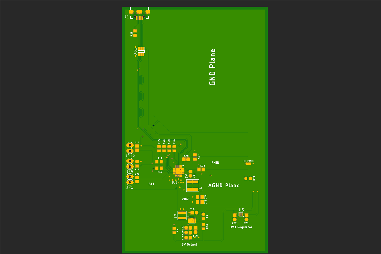
I'm an embedded systems engineer and i'm actually designing a power supply PCB using BQ25895. I already did some PCB layouts but never as complex as this one, that's why I'm asking for reviews on this forum.
I'm going to soldering it using a reflow oven, that's why there aren't any components on bottom side, I also added some texts on the PCB to help understanding the PCB.
The first big point result as a misunderstanding of the datasheet, I don't know if I should use PMID output or use the switched output (SW, near L4). PMID is only active in "Boost mode", that's why I connected a TPS61232 as a Step-Up converter to the SW output to provide 5V (up to 5A).
To prevent any fails I put a 0 Ohms resistor to get access to PMID plane.
Then, those are the points whom I'm not comfortable:
- Has my PCB enough copper to dissipate the heat and handle current flows ?
- Is my PCB well designed to prevent EMI and ground loops ?
USB has a protection circuit (ECLAMP2122s) to prevent from TVS, ESD and EMI troubles and USB lanes are impedance tuned.
Here, you can find a zip file with:
- Gerber Files
- Capture of TOP and BOT gerber
- PCB Schema
Thank you for reading.
BQ25895_DesignBlock.zip


