This thread has been locked.

If you have a related question, please click the "Ask a related question" button in the top right corner. The newly created question will be automatically linked to this question.

TPS650864: TPS6508641 Power drop

Part Number: TPS650864
Other Parts Discussed in Thread: USB2ANY, TPS650860EVM-116, IPG-UI, CSD87381P

Hi

I designed the TPS6508641 for ZU4EG.

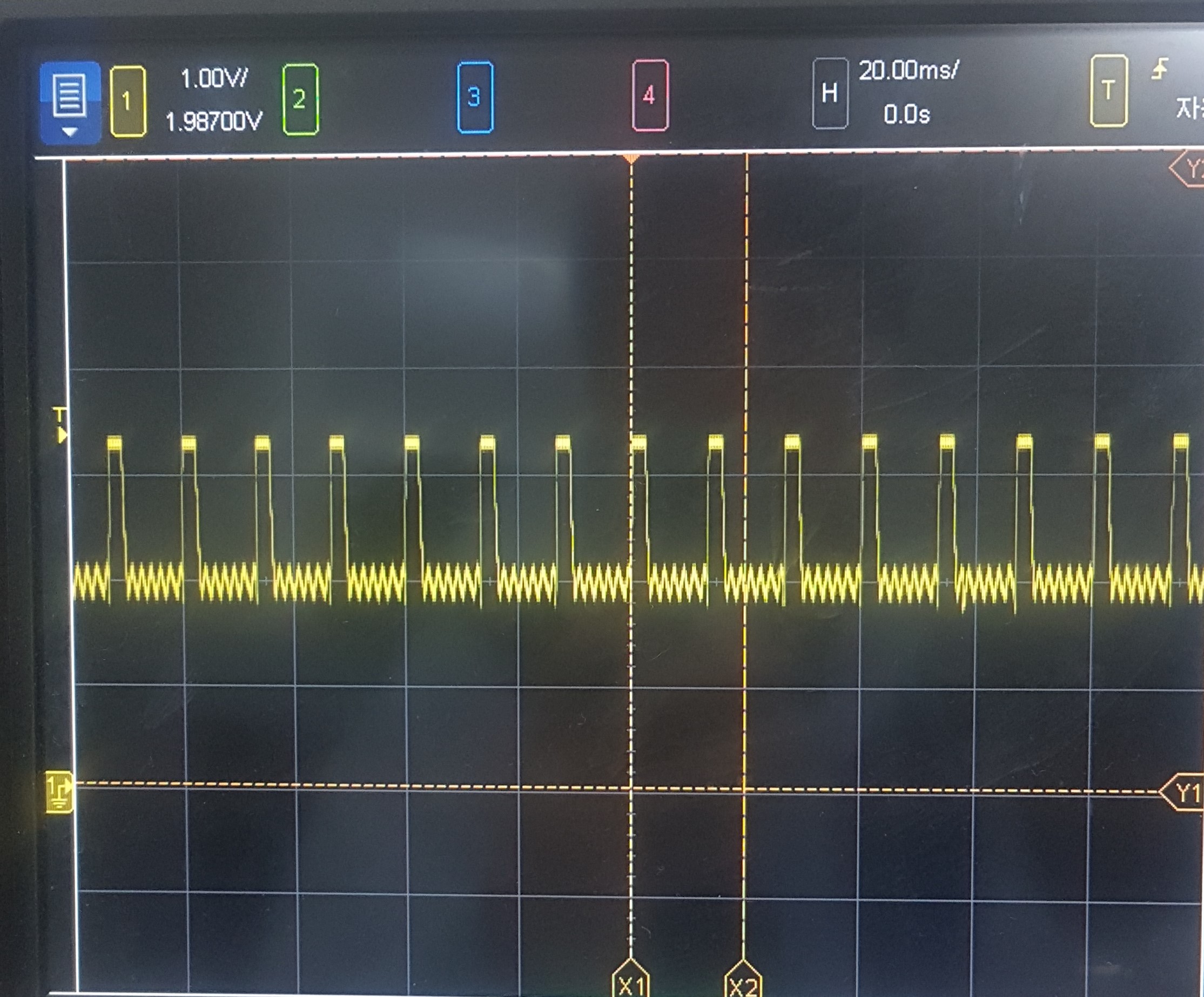
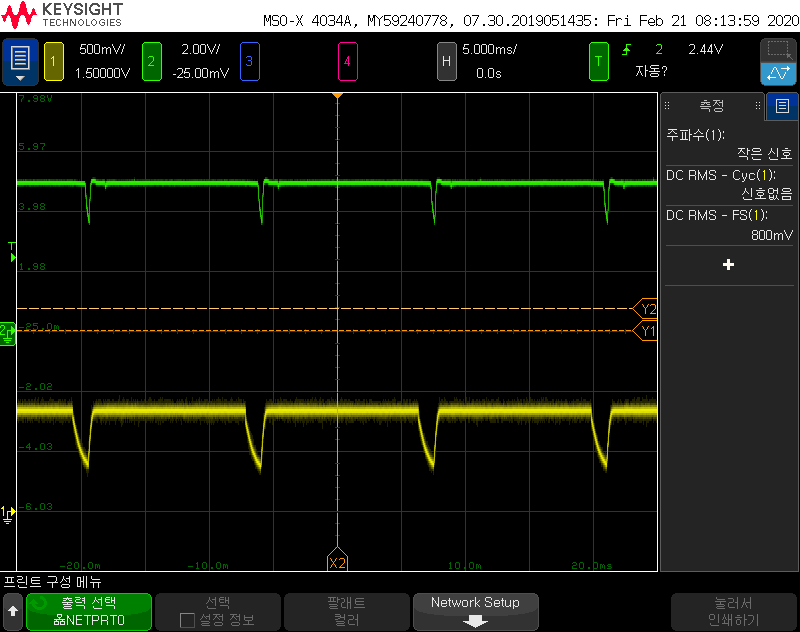
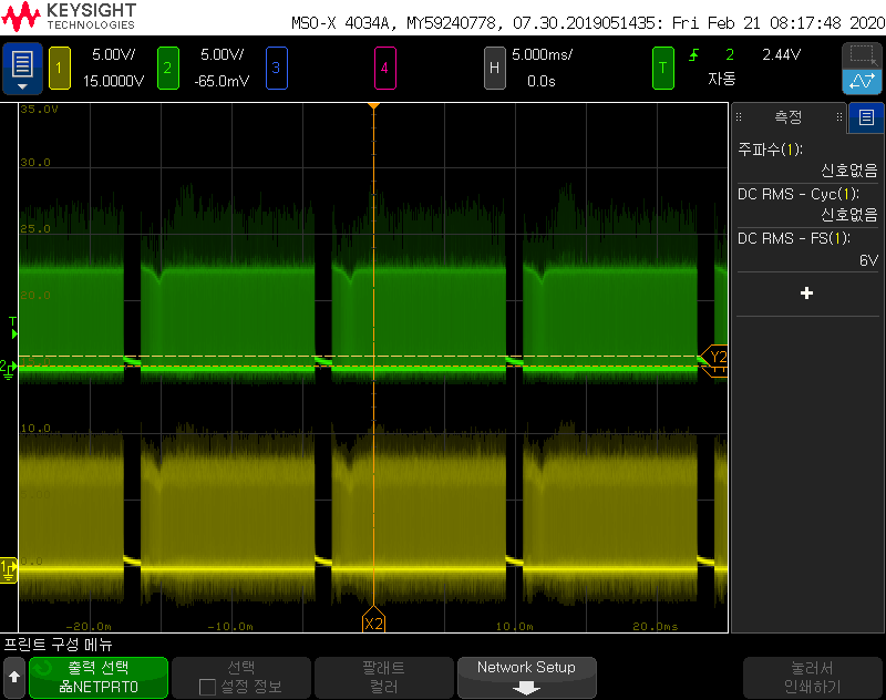
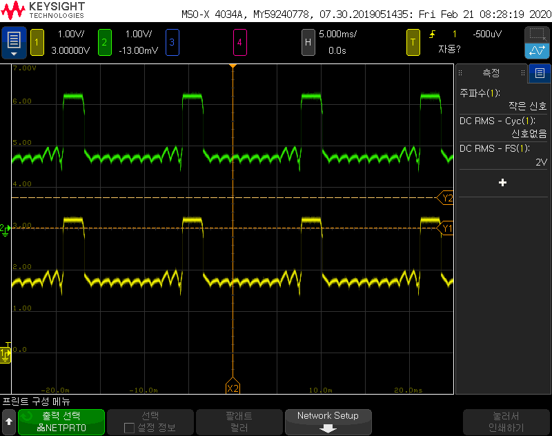
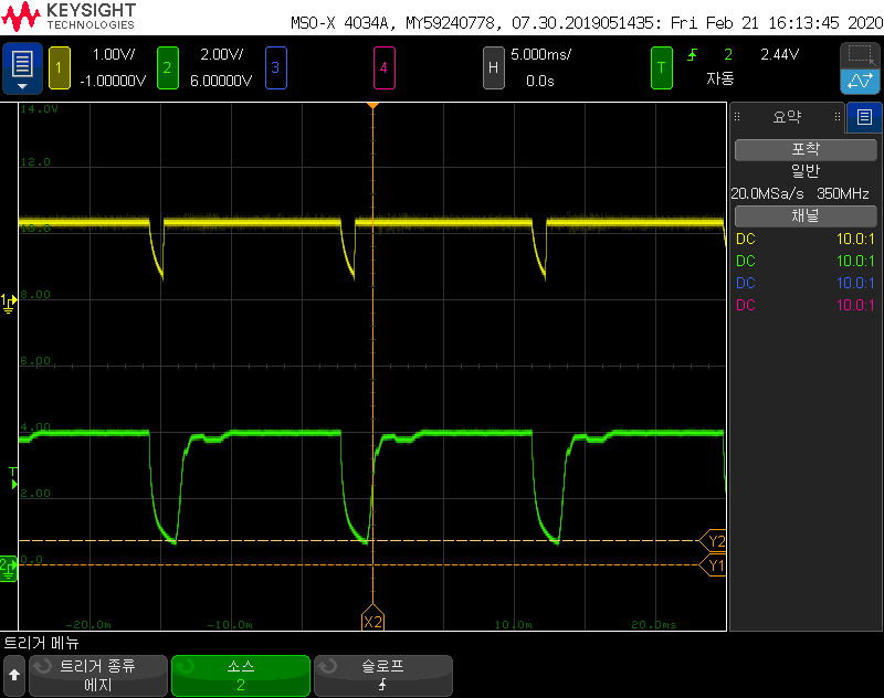
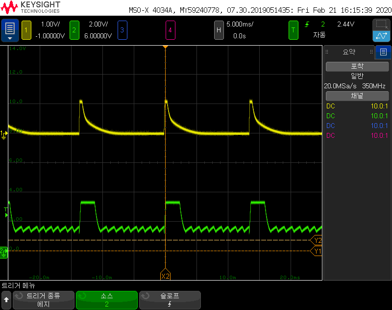
When I power up, buck2(0.85V) drop as shown below.

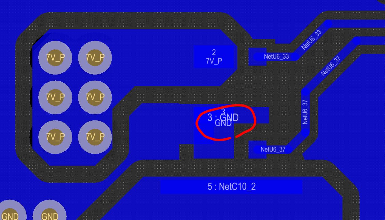
I attached my schematic.

4503.PMIC.pdf

One thing the sure, buck1 output is  normal.

but when Buck2 output occur, Buck1 also dropped like the above picture. 

  • Hi Geonwoo,

    I am concerned by the CTL3 waveform; it appears to have a 10kΩ pull-up to LDO3P3 and then an external connection to PS_FP_PWR_EN_O. Ideally this signal is either high or low. Do you have any idea why PS_FP_PWR_EN_O is behaving this way?

    Beyond that, it is hard to tell but I have some suggestions. The PMIC monitors all of its regulators for power fault condition (over voltage / under voltage). If any rail has a power fault, the PMIC performs emergency shutdown, disabling all rails. To confirm, BUCK2 is not reaching the 0.85V point, but rather stuck around 0.72V? Looking at schematic, I see around 44 uF of capacitance for BUCK1/2/6 - can you try increasing this to 88 uF and see if you have improvement? Ripple voltage with such little capacitance may be an issue (it is why you see the overshoot on BUCK2 most likely).

    Do you have ability to use I2C to talk to the part? For example with USB2ANY + IPG-UI, or TPS650860EVM-116. If so, you could use I2C to read the SHUTDNSRC register to see why the PMIC is performing emergency shutdown.

    If none of that is available, then next step would be to take scope shot of each rail in the power up sequence (Figure 6-11) and see where the measured does not match the figure.

  • Thank you for your reply.

    Unfortunately I can't use I2C of PMIC in current design. 

    And I added a capacitor as you say.. Buck ripple was reduced, but voltage drop remained the same.

    I have a question.

    In pcb artwork, i saw CSD87381P in detail.

    Pin3(PGND) is connected thin, is this the cause of problem?

  • I removed external connection to PS_FP_PWR_EN_O , and then CTL3 is now 3.3V. 

  • Thank you for confirming the CTL3 behavior is linked to issue from input, not PMIC.

    Regarding PMIC reset:

    1. The layout will most likely cause a current limit issue. The SW2 and PGNDSNS2 are differentially used to measure the voltage on the LS FET. If there is a large series resistance, then the PMIC will think there is a large current because the voltage will be large. You could try removing the ILIM2 resistor entirely but it may still not be enough. To confirm that it is a current limit issue, I would recommend taking scope shots of the SW node and check the voltage when the LS FET is on. You can then use this with the "Current Limit" equations on pg 49 of the datasheet.

    2. Were you able to confirm that BUCK2 voltage is measured at approximately 0.72V? Note: this is a valid voltage for the core rail, which makes me curious if there is any I2C traffic doing this transition. For example, make sure there is no DC offset on the oscilloscope

    3. Can you provide scope shot showing the I2C lines at the same time as the image from the first post? If FPGA is adjusting the voltage down to 0.72V, then this is expected behavior. If the actual voltage is measuring 0.85V, then no need for this step.

    4. Can you confirm where the power up sequence you are seeing is different from that shown in Figure 6-11? The BUCK2 voltage (as well as every other regulator) will turn off in the event of ANY power fault, so you need to identify when the power up sequence is different.

  • Thank you very much for your reply.

    I said that before, buck1 output is normal. That's true when PMIC power-up sequence only operate till BUCK1.

    But when the next step of power-up sequence operated, BUCK1 output seems to repeat turn on/off as well as BUCK2.

    1, I removed all ILIM resistor and short to 0 ohm as you say, but PMIC output related to buck remains the same.

    CH2(GREEN) DRVL2, CH1(YELLOW) SW2.

    2. BUCK2 voltage is measured 0.85V in current board. The board, measured at 0.72 V, is dead..

    3. CH2(GREEN)  I2C DATA, CH1(YELLOW) I2C CLK.

    The operation is seems to same as CH4 input in former.

    4. As i mentioned, buck1 output is normal. But if the power-up sequence is operate continuously, buck1 and buck2 are malfunction.

  • Ok, to confirm:

    If CTL3 = short to GND, BUCK1 can power up and there is no restart occurring, so at least BUCK1 is stable.

    With CTL3 pulled high, restart begins occurring. However BUCK2 voltage is 0.85 V on current board so it does not appear to be the problem. They do not appear to be malfunctioning. Most likely there is some other item causing an emergency restart, which causes both regulator to shutdown.

    There was no scope shot with other BUCKs, is BUCK5 not powering on? It should turn on at the same time as BUCK2. If BUCK5 is not powering on, then that would likely be the cause of the power fault. If BUCK5 is powering on as expected, then you need to scope the next voltages in the sequence to see if any of them are having problems.

  • I attached picture buck5, buck6, buck3, buck4. (sequentially as below.)

    buck6 is 1.8v but the result is approximately 4v.

  • Hi Geonwoo,

    BUCK6 = 4V would cause a power fault (after a 10 ms mask during power-up) which would result in the shutting down that you see. 

    I would recommend looking at the switch node of BUCK6, and potentially add more capacitance if you did not try already. The next basic goal should be determining if the regulator is causing the overvoltage or whether some external supply is pulling this net up.

  • Hi,

    I found out a new fact.

    I change PMIC VSYS voltage from 7V to 5.7V, the deivce is operate in normal. All Bucks are operate in normal. (But Buck1 voltage is not 5V but 4.8V.)

    But when i change VSYS voltage more than 6V, the device is malfunction. All of the previously described phenomena appear.

    I think it is more like pcb artwork problem than circuit problem.

    Buck1 is most suspicious. The CSD87381P datasheet states that the higher the input voltage, the higher the power consumption.

    As I mentioned, Buck1 Gnd pattern width is 0.15mm In current pcb artwork.

    So Buck1 is most suspicious but i can't debug because CSD87381P is so small to do wire work.

    I would really appreciate your device. 

  • Hi,

    What is suspicious about BUCK1 operation? It seemed to be regulating at 5V with no issue in the scope shot provided. The layout is a potential problem but I thought it was clear that BUCK6 was creating the issue?

    The higher the Vin, the larger the ripple current would be, so maybe that has an impact.

    Have you looked at the switch node of BUCK6 yet to see if the >1.8V is due to switching or from external supply?

  • I don't know why Buck6 is over 4V when board is malfunction. But if VSYS is 5.7V, the output is 1.8V.

    The reasons i suspect Buck1 are.

    1. This schematic is the same as before the modification. Only artwork changed. So i don't doubt the schematic and ICs mounted on PCB.

    2. If VSYS is over than 7~8V, the the switching node output inductor of Buck1 is burns out. In previous PCB, all Bucks outputs were no problem.(even VSYS was 10V in previous PCB) 

    3.So I'm most suspicious of Buck1, and I think the thin GND pattern of that is the problem. I'm just in doubt this. But there is no way to verify it.

    Thank you.

  • Hi Geonwoo,

    In order to rule out BUCK1 issue, can you apply external 5V to the 5V_P after VSYS has been applied (while the part is resetting)?

    The BUCK1 seems to be operating correctly (regulates at 5V until the part shuts down), but one potential is that maybe the current limit is kicking in (due to the large effective resistance of the low side FET) and then the input to BUCK3/4/5 is going low during their startup.

    If this causes the board to be stable, then the GND trace is most likely the issue. If the problem persists, I would recommend zooming in to the switch node of each buck and seeing if they are acting abnormally.

  • Sorry, I didn't understand you said.

    What is the meaning of external 5V? is it BUCK1 output?

    I don't understand exactly, but It is possible to add an external 5V with power supply.

    There is an additional confirmation.

    We made ten PCB Board.

    One of them operate in normal. When VSYS voltage is under 6V.

    And four PCB board are not operate under 6V. But When VSYS voltage is over 10V, these are operate in normal.

    And then these work continuously regardless of the VSYS change... But Power consumption is so high about twice.

    The others are not operate regardless of VSYS change. The result are the same as before.

    I really want to find the cause.

    Thank you.

  • Hi Geonwoo,

    Regarding BUCK1 test, you are interpreting correctly, my intent was to connect an external 5V power supply to the 5V_P net to see if the system is more stable without BUCK1 being over-ridden by external supply.

    With such variation in board performance, my first instinct is that there may be soldering issues. Checking this would generally involve checking resistances on good vs. bad board when no external power is supplied. 

    You need to do a detailed analysis of the power up sequences, trying to figure out where the voltages are not reaching the intended voltage and then analyzing the switch node if it is a buck regulator (https://training.ti.com/sites/default/files/troubleshooting-buck-design-issues.pdf) or determining if the Vin is stable for LDOs.