


Part Number: BQ25703A
Other Parts Discussed in Thread: TIGER, CSD17551Q3A, CSD17551Q5A
Hi
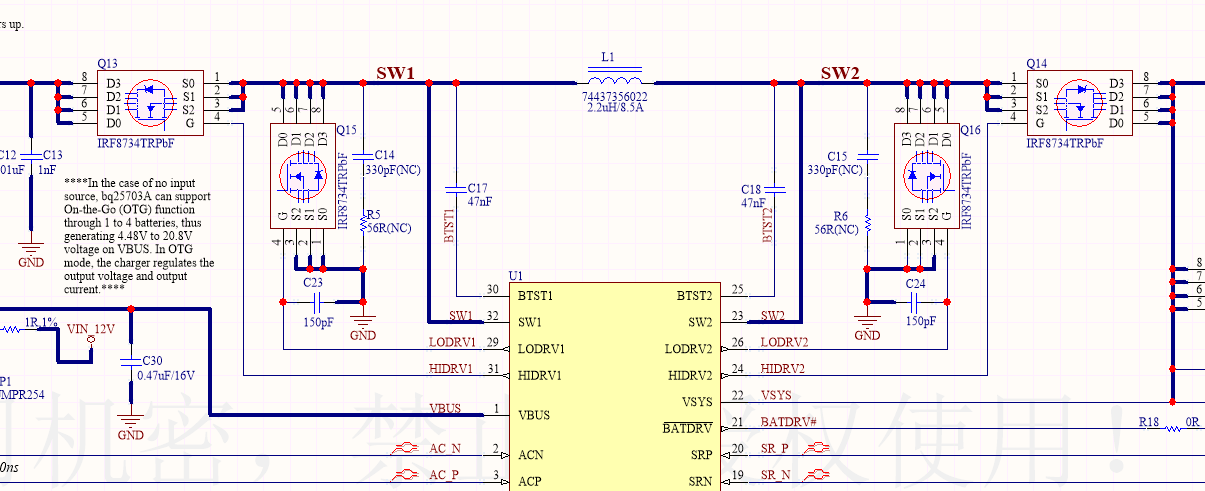
My customer designed with BQ25703A. BQ25703A works in Boost Mode, input voltage 12V charges 4S1P LiFePo4 battery (maximum 14.6V), registers setting as below:
Charge Option 0 820E
Charge Current Register 0800
Charge Voltage Register 3900
OTG Voltage Register 0000
OTG Current Register 0000
Input Voltage Register 2100
Minimum System Voltage 2D00
Input Current Register 3C00
Charge Status Register B400
Prochot Status Register 0040
Input Current Limit In Use 3C00
VBUS and PSYS Voltage Read Back 8410
Charge and Discharge Current Read Back 1E00
Input Current and CMPIN Voltage Read Back 3900
System and Battery Voltage Read Back B2B1
Manufacture ID and Device ID Read Back 7840
Device ID Read Back 1078
Charge Option 1 9210
Charge Option 2 02B7
Charge Option 3 0000
Prochot Option 0 4A54
Prochot Option 1 8128
ADC Option 2000
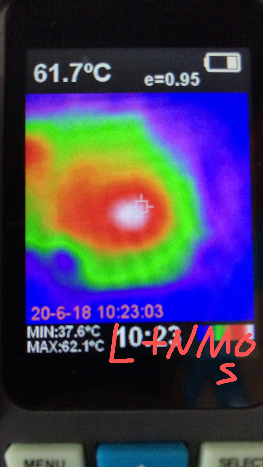
VIN=12V, VBUS=12V, VSYS&VBAT (the voltage slowly rises to 14.52V), the charging current is 2024mA, and find that the inductance (L1) and two MOS tubes (Q14&Q16) and BQ25703A chip in the boost mode are very hot, The larger the charging current configuration is, the hotter it is, when the charging current is 1024mA there is no problem.
NMOS tube selects NTMFS4833NT3G, RDS(ON)= 2.0mR@10V, Id(max)=191A, SO-8 FL package;
Inductance: 74437356022 2.2 μH, 8.5 A, 0.0203ohm;
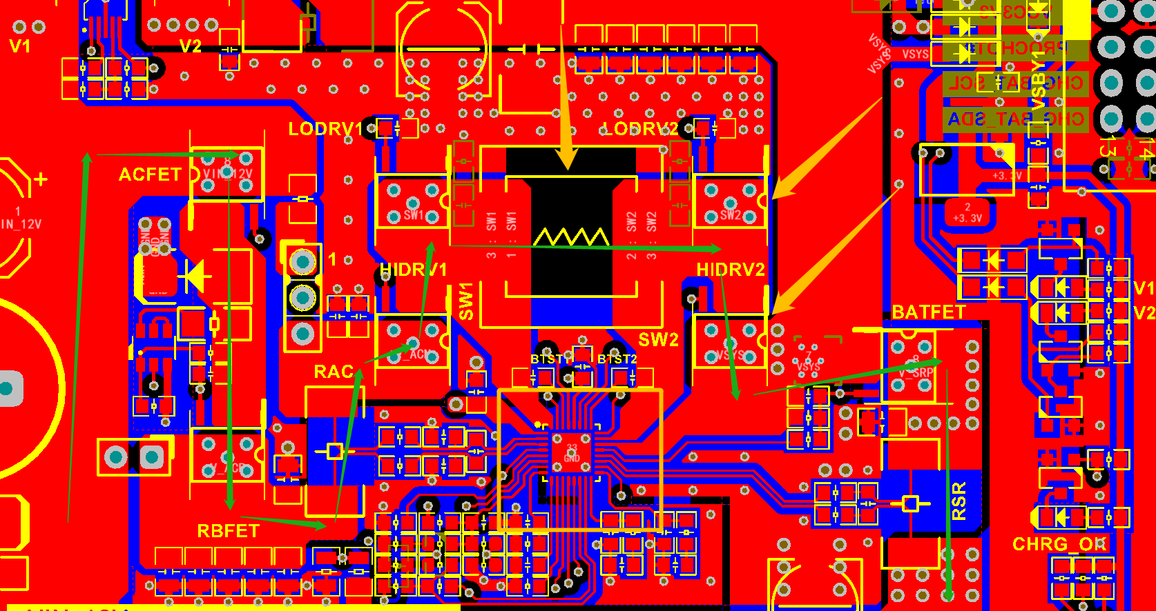
The following six pictures are SCH, PCB, signal waveform and heat map, please help check.


Thanks
Star


