This thread has been locked.

If you have a related question, please click the "Ask a related question" button in the top right corner. The newly created question will be automatically linked to this question.

WEBENCH® Tools/TPS40210: negative voltage to negative voltage switcher at 6A.

Part Number: TPS40210
Other Parts Discussed in Thread: TLV172

Tool/software: WEBENCH® Design Tools

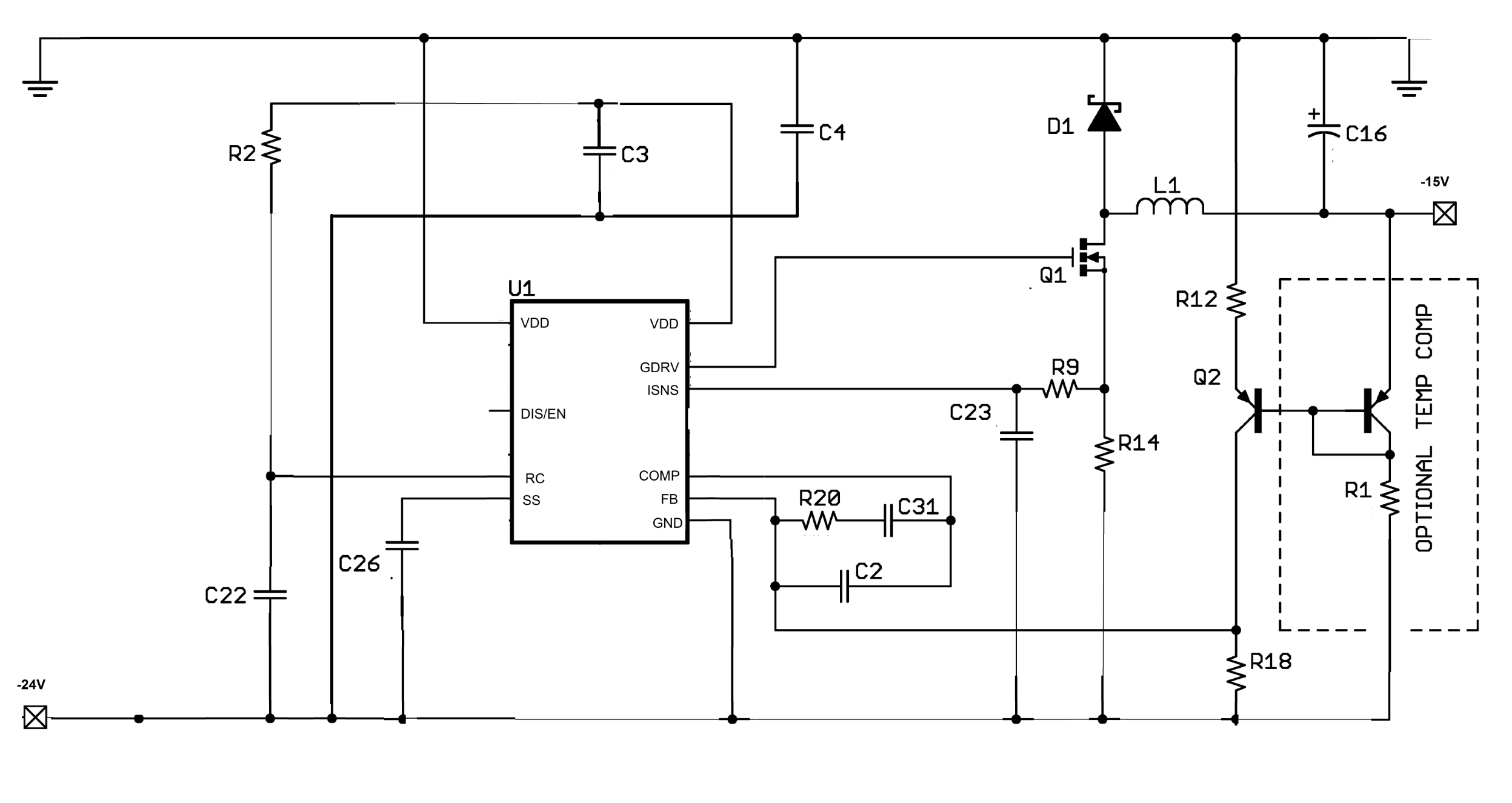
I am trying to  design a -24V to -15V switcher that can deliver up to 6A. Years ago Peter James Miller provided a topology which used the TPS40210 to generate a similar design but didn't provide any insight on how to calculate the R's and C's.

Also Webench does not accept negative input or output voltages for the TPS40210.

  • Hi Burt,

    What you mentioned must be a negative Buck, and the IC's GND reference pin should be tied to the input negative rail, as shown in the attached drawing, which I modified from an existing design with a different part.  The power stage (inductor, MOSFET, diode, and input/out cap, as well as current sense resistor) are calculated as the in a regular buck converter.  The Feedback needs level shift to sense the output voltage.   The feedback voltage is the voltage across R18, which has the same current as R12, and the R12 current is calculated by 15V/R12.  The pair npn bipolars cancels temperature coefficient of the effects of the npn BE junction.

    Hope this help.

    Youhao Xi, Applications Engineering

  • Hi Youhao,

    Yes, your answer helps, especially the part about calculating the rest of the values as a regular buck regulator.

    I am uncertain about some things still:

    1. What is "COM" in your schematic connected to? It looks like ground.

    2. I calculate Risns (R14) to be about 8mOhms. Is that about right?

    3. I have R2 = 200K to get 1Mhz switching frequency. This allows me to keep the L1 inductor to 6.8uH. Did I do this calc right?

    4. Peter James Miller in his original post from 2011 suggested an inverting opamp in place of the npn bipolars to generate the input to FB. I have a TLV172 with 4 resistors but don't know how to calculate what the resistor values should be.

    5. How should the FB resistor divider values be calculated?

    Thanks,

    Burt Hashizume.

  • Hi Burt,

    Very sorry the drawing that I posted has errors that were leftover when I modified an existing drawing for you.  C3 and C4 should reference to the IC GND, or the -24V input rail in this case.   The COM GND symbols should be deleted. Here I attach an updated drawing.  Sorry for the confusion.

     (2)  How do you calculated it?  It is a buck converter and the inductor dc current should be the load current.  Under 1MHz 6.8uH, the ramp current is about 0.8A, leading to a peak inductor current of about 6.4A.  Then the current sense resistor should be about 16mOhm.  

    (3) It should be okay if the timing capacitor is chosen to be 68pF according to the datatsheet frequency curve.  However, to me 1MHz is too fast for this 90W design.  You will not have good efficiency, given the fact that the circuit is hard switching. Recommend to reduce to below 400kHz.

    (4) I haven't see that suggestion.  We started to support the TPS40210 since Feb 2017.  The pair pnp transistors should be a simple way to perform the level shift Vout sensing. 

    (5) It is very easy to select these resistors. Refer to above drawing, R18 and R12 see almost the same current, if the bipolar HFE is >>1.   The current through R12 is Vout/R12. The two PNPs just cancels the effects of Vbe and temp coeff of it.  The the VFB = R18 x (Vout /R12).  You need to choose these resistors such that VFB=Vref of the TPS40210 when Vout reaches the setting point of 15V.

    Hope this clarifies.

    Thanks

    Youhao

  • Hi Youhao.

    2. I used eqn 16 for calculating Risns. D = -0.655, Visns = 150mV, Iout = 6A, Fsw = 1Mhz, and L = 6.8uH. I get about 8mOhm. If D = +0.655, then Risns = 9mOhm.

    3. Figure 2 shows that 1Mhz is within the acceptable range for D = +0.655. I'm going for a faster switching frequency in order to keep the inductor value and size smaller. There doesn't appear any other pro or con argument for different switching frequencies.

    4. I'm attaching part of Peter James Miller posting from Feb, 2011. The diagrams don't appear to copy over but you can read that Mr Miller believes using an opamp provides higher accuracy. Maybe you can find his original posts to see the diagrams.

    "Feb 25, 2011 3:47 PM

    In reply to Peter Miller13277:

    There is an error in the above circuit's current mirror.  The base topology is correct, but the circuit to reflect the voltage to the low-side rail is not.  I will correct this in a new post shortly.

    Peter James Miller

    New Product Development Engineer

    Power Management - DC/DC Solutions - High Performance Solutions

    Member Group Technical Staff 2008

    Here is the corrected circuit

    Since these are external MOSFETs and the two MOSFETs of the current mirror will have slightly different Vds voltages, they wont have perfect matching, so the 5V precision will be a little wider than normal and R3 should be sized to to keep the Vds of the two FETs of the current mirror as close as possible without dropping below their threshold voltage.  Using higher voltage small signal MOSFETs (such as a 60 - 100V MOSFET) will decrease this effect.  A Cascode would also help, but would improve the accuracy, but involves 4 additional MOSFETs.

    An alternative would be to use a differential amplifier across Vout to reflect Vout to -Vin.

    A few more components, but this offers much better accuracy.

    Peter James Miller

    New Product Development Engineer

    Power Management - DC/DC Solutions - High Performance Solutions

    Member Group Technical Staff 2008"

    5. I am not an analog circuit designer so I don't follow what you are saying regarding HFE, Vbe, etc.

  • Hi Burt,

    You cannot use the datasheet equation to calculate for this case. It is a buck circuit now, and the datasheet is for a boost. Please apply buck formula for the current calculation.

    Regarding the level shift circuit, I am proposing biplar not MOSFETs. You can find paired pnp for better matched Vbe and they will cancel each other without affecting your output accuracy.

    Thanks,
    Youhao
  • Hi Youhao,

    Now I am even more confused.

    The TPS40210 is a boost controller. There are no buck formulas in the datasheet with which to calculate anything. I understand we need a boost controller to convert a more negative voltage to a less negative voltage but I thought all the other values were calculated "normally" ie using it as a boost controller.

    I also don't understand your phrase of "ramp current".

    Also is 1Mhz switching frequency OK. If not, why is it better to have 400khz switching frequency?

    I am willing go use bipolar transistors, matched pnp, but I don't know how to select them nor how to calculate the surrounding resistor values.

    Thanks for your help.

    Burt Hashizume.