This thread has been locked.

If you have a related question, please click the "Ask a related question" button in the top right corner. The newly created question will be automatically linked to this question.

UCC24612: UCC24612 PWM fail

Part Number: UCC24612

Hi,

I follow the UCC28780EVM for an adapter design, and UCC24612 is used as the secondary SR driver.

I found the PWM_SR failed for the second pulse as below. 

Could you help explain why the second pulse failed?

CH2:VDS; CH3:VGS; CH4:Ipri
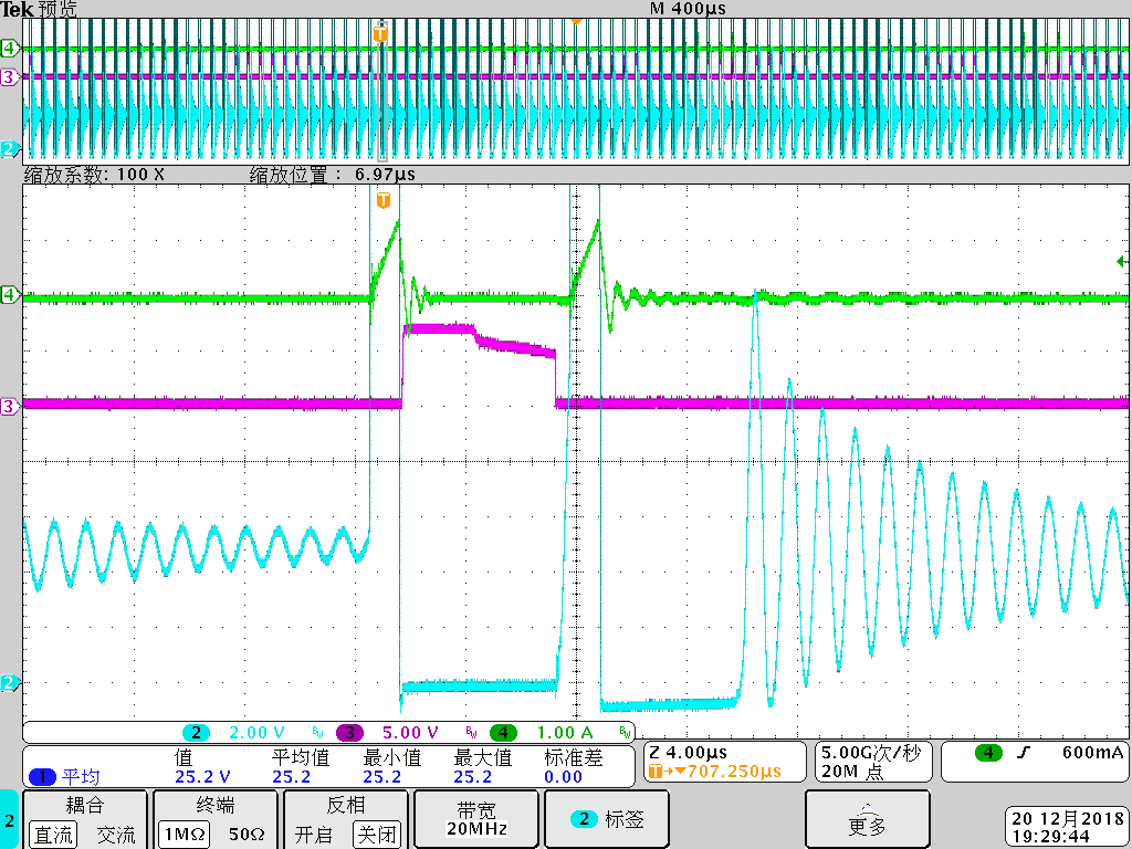
  • Hello Eleven,

    I wonder if VDD had enought voltage on the second pulse. Could you take a look at VREG and VDD along with these waveforms. It could be that you the design may not have enough capacianctance on VDD and VREG.

    Regards,

    Mike
  • Hello Eleven,

    One of my colleagues discussed the issue with me that you were having the UCC24612 and he let me know that in burst mode the UCC24612 could actually skip pulses under certain conditions.

    From DS page 18:

    “UCC24612 sets up the off blanking timer based on previous cycle's SR off time. By choose 70% of previous switching cycle's SR off time, the off blanking timer is maximized to prevent any false triggering.”

    >Maximum off time is 3.68us.


    From DS page 20:

    If for any reason the off blanking time expires after the SR body diode conduction, the SR turning on is skipped for the switching cycle. This is because when the SR conducts, it conducts with a minimum on time, if the blanking time expires at the end of the SR conduction time and converter operates in the CCM condition, there is a good chance to cause shoot through the endanger the converter.


    Since the previous burst happened some 100us earlier, controller sets the off-time blanking to 70% of 100us, except it maxes out at 3.68us.

    Since this burst’s 2nd pulse on-time is only about 1.5us, the off-timer (3.7us) from the 1st pulse has not expired yet at the 2nd pulse turn-off point so it triggers the response highlighted in green. 

    The 1st pulse of the next burst then works okay, but it’s 2nd pulse gets the same treatment as above.

    That’s why you sometimes see a missing SR at the 2nd pulse of a multi-pulse burst.

    Regards,

    Mike

  • Hi Mike,
    Thanks for your detaled analysis.
    So it is a normal phenomenon for UCC24612 in this mode, right?

    BR
  • Hi Mike,
    In the page 14 of datasheet, it say "However, this forced minimum on-time can allow current that transfers the energy from output to input and
    reduces the overall converter efficiency."
    In this paragraph, I think it wants to say the importance of minimum on-time, and it could avoid the mistrigger of turn-off.
    But for this sentence, I can't understand what it wants to express.
    Could you help explain what is the meaning?
    Thanks!

    BR
  • Hi Mike,
    In the page 15 of datasheet, it say "This high current slope could cause large negative current due to long propagation delay. Furthermore, the delay caused by discharging the SR MOSFET gate from full voltage to its threshold level introduces another delay, further increasing the negative current.."
    What is the meaning "large negative current"?
    What is the influence that the large negative current will bring?
    Thanks!

    BR
  • Hello Eleven,

    I can not find this section in the UCC24612 data sheet on page 14.   I did find this paragraph that explains what your are interested in. 

    For certain applications, this delay is essential for appropriate operation. In Active Clamp Flyback, especially

    when the primary side switches are using Si based super junction MOSFET, due to the large nonlinear junction

    capacitor, the SR often sees a leading spike current, follow by the real conduction current. Normally, a prolonged

    minimum on time can override this spike to make the circuit operate normally. However, this causes large

    negative current that transfer the energy from output to the input and reduces the overall converter efficiency. In

    UCC24612, two different versions are created. UCC24612-1, the SR driver with inherent short turn on

    propagation delay (70 ns typical) can be used with the converter needs shorter delay, such as standard Flyback

    converter or Active Clamp Flyback covnerter using GaN MOSFET as main switches. UCC24612-2, the SR driver

    with added 150-ns turn on delay, to further ignore the leading edge spike, can be used with Active Clamp

    Flyback with Si based super junction MOSFET as the main switch or the LLC covnerters.

    Does this help?

    Regards,

    Mike

    ---------------------------------------------------------------------------

    Hi Mike,

    In the page 14 of datasheet, it say "However, this forced minimum on-time can allow current that transfers the energy from output to input and

    reduces the overall converter efficiency."

    In this paragraph, I think it wants to say the importance of minimum on-time, and it could avoid the mistrigger of turn-off.

    But for this sentence, I can't understand what it wants to express.

    Could you help explain what is the meaning?

    Thanks!

    BR