This thread has been locked.

If you have a related question, please click the "Ask a related question" button in the top right corner. The newly created question will be automatically linked to this question.

UCC28950: secondary winding and choke connection

Part Number: UCC28950

Hi!

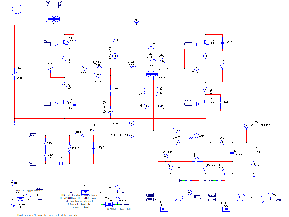
Iam designing 7kwt converter using ucc28950 and i whant expert advice  if i can leave secondary windings separate before dc choke (end and begining of two secondaries are connected in datasheet),put wires form secondaries right throug a choke and connect them togeather right after a choke on a filtering capacitor? 

reason why i ask if it will work fine or not is that i have to strip 150 separate emalled copper wires in order to connect them togeather at that point before a choke,and thats a peace of a work,which is not the joyfull one.

the other part of question may be: does each secondary wire carry the whole output current?
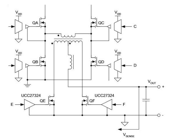
  • Hello Slavko

    That's an interesting idea and I had not seen it before. So - I ran a few simulations to see what would happen - if you have PSIM I can share the files with you.

    1/ To a first approximation your idea will work

    2/ In my sim (12Vout at 60A - nominally) with the 'normal' circuit you show above the output inductor RMS current was 56A. In the modified circuit the current does of course share equally between the two inductor windings but the RMS currents were 39A in each winding.

    3/ There is a duty cycle loss in the modified circuit - my 12V output dropped to 11V. This is due to the need to transfer the current out of one winding and into the other winding at the end of the freewheeling interval. This would have to be taken account of when designing the main transformer to make sure you had enough effective duty cycle range.

    4/ Have you considered using single winding secondary with a full bridge rectifier. The SR signals (OUTE and OUTF) can be used to drive SRs in a full bridge - with appropriate high/low side drivers of course.

    5/ Have you considered using a foil secondary ?

    6/ Your inductor has to have two windings on it which will take up more space than a single winding and is there a production method available to make this design in quantity ?

    7/ The normal way to tin multiple windings (even 150) is to get a solder pot and dip the end of the wire group into it - we used this method frequently when I worked at a PSU manufacturing plant some years ago.

    8/ How much work will this actually save you ? you still have to tin the 150 wire group as it exits the two winding inductor rather than as it exits the transformer. If you have a single winding inductor you can wind it with really heavy copper wire because most of the current is DC and skin effects may not be a big problem.

    Anyhow - it is an interesting idea - let me know if you want the files. Here are a few screen shots of what I did. Please double check that I got the circuit correct.

  • Hi Colin!
    Iam deeply touched,that you devoted that much time to make that simulation and you payed attention to me.
    i didnt expect that much care.
    if you say that voltage drops due to the loss of duty cycle,and summ of the currents in inductorwill rise all that is unaccaptable then. idea does not worth it,especially when you said,that within inductor a thick solid wire can be used instead of litz.then it does not add much work.
    i have thought,that there is big magnitude of pulsating current in the inductor,so skin effect should increase ac resistance of the wire.but your words made me hesitate about this. i should read more about this maybe later,make some experimets tofind out whats happening there...
    anyway i am very happy that you responded to me,and helped me alot. Thank you,Colin!
  • Hi Slavko

    You are welcome and thanks for the feedback.

    You asked an interesting question ! and I had the basic PSIM file already to hand, I just had to make a few small modifications :-).

    Most of the inductor dissipation will be due to DC loss with a smaller component due to the high frequency ripple - skin effects are not too important in the normal connection although they would be high in the dual winding configuration because - as you note the currents would be pulsating.

    Let us know how you get on.

    Regards
  • hello collin
    Could you pass me that simulation file in psim?
    I designed with ucc28950 but I have had some problems when implementing the feedback loop, and the average model of this in pspice has not worked well for me
    thank you very much.
  • Hello Yelsing

    Here it is. Please note that this is a very simple model which runs open loop - you can see that I have used a simple collection of oscillators and gates to generate the OUTx signals - there is no UCC28950 involved. I use this to look at basic questions about the PSFB rather than at the behaviour of any controller. Nevertheless you may find it useful.

    Please let me know if the link does not work, if that happens I can email the file directly to you.

    Regards

    Colin

    /cfs-file/__key/communityserver-discussions-components-files/196/7633.PSFB-3kW_2C00_-12V_2C00_-two-winding-choke-PSIM.sch

  • Colin,can i ask you 2 more questions about ucc28950 application?

    1)could current sensing transformer be moved from the supply rail to the transformer's primary? will controller operate correctly with ct in the power transformer primary? ofcoure current transformer signal will be rectified using full bridge rectifier.

    2)should dc blocking capacitor be placed in series with transformer's primary to prevent core saturation in the situation when pwm duty cycle changes. so when previous duty cycle is different from the current,transformer does not get a dc bias that can saturate the core?

    Thank you!
  • Hello Slavko

    Yes it is also possible to place the CT in series with the power transformer primary winding. In this case the CT primary current will be bi directional and this will require a full bridge rectifier on the CT secondary to produce the unidirectional CS signal that the controller needs. As you note. The concerns about CT saturation are valid. I'm afraid I haven't any direct experience of this.

    I would recommend either a DC blocking capacitor - but they are likely to be rather expensive. T with sufficient margin.

    • If the CT is in series with the input DC line then it senses both the ‘proper’ transformer primary current when diagonal switches are on AND it senses any shoot-through current if for some reason both the A and B or C and D switches are on simultaneously. In this location, the current in the CT primary is unidirectional and a single diode rectification is all that is needed to produce the unidirectional CS signal that the controller needs. The main concern is that you have to allow sufficient volt/seconds for CT core reset. The CT must be placed directly before the power stage as shown in my sim. The input capacitor for the bridge must be placed across the voltage source - I didn't need one in my sim of course because the output impedance of the source was zero.

    • I would note two subtle effects if the CT is in the transformer primary –

    o First, the CT primary will have a very significant common mode signal on it as the bridge switches the transformer polarity around. This will couple noise on to the CS signal through any stray capacitance between the CT primary and secondary (including any capacitance associated with the PCB tracks). If I were doing this, I would place the CT in the CD (Active/Passive) leg because this leg will maintain ZVS down to lower currents than the AB (Passive/Active) leg. Loss of ZVS will give higher dv/dt rates and increased currents in stray capacitance.
    o Second, the CT will occupy what is ‘prime real estate’ on the PCB and may force the layout to have higher stray inductances and capacitances in the MOSFET circuits than would otherwise be the case. The switched node at the CT primary will certainly be larger than it would be if the CT were not present and larger switched nodes will have higher capacitances to other parts of the circuit leading to increases in system noise and EMI. The added stray inductance can be placed in series with the main transformer where it is relatively harmless (it adds to transformer primary leakage inductance)

    Given a choice – I would place the CT in the input DC path.
    You may also find the article at www.ti.com/.../slup348.pdf of interest.

    Regards
    Colin
  •  it seems that i have found a reason of output CD duty cycle issue!
    i was experimenting and i found that capacitor on CS signal was cracked.when i was soldering around him,he broke apart. when i replaced him with a normal one extreme duty cycles dissapeared! but still it gets to 38%. is it normal for this controller to have 38% or 62% duty cycle those are signals from both gate transformers. why is that so one leg is allways 50% and other change ist duty cycle?