


Part Number: AM625SIP
Tool/software:
I have a PDN related question about AM625SIP. I went through most of the documentation HW related available online, and am pretty confident we can work with it. We would use 6 layer PCB and closely space the PWR/GND planes respectively.
What I am trying to evaluate now is the following:
Implementation Examples and PDN Targets Table 7-6, mentions max L per cap is <1.5nH for AM62xx, admittedly it is not the SIP, but a similar table for SIP does not exist.
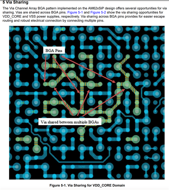
Another app note, covering the fanout, AM62x SiP Escape Routing for PCB Design, section 5 Via Sharing, shows a way how to fanout the VDD_CORE and how the actual footprint of the BGA has been thought/designed with via_sharing in mind. However, traces shown on the image(snapshot from above app note), already add >1.2nH in trace itself leaving almost an impossible margin for the PDN(sandwich of pwr/gnd + decoupling).
It seems like two recommendations, from different perspectives, contradict each other.
Do you have internal success with "via sharing" or is the PDN target set to be too cautious OR a SIP variant can be more "relaxed" in terms of PDN?”
