[FAQ] AM625 / AM623 / AM620-Q1 / AM625-Q1 / AM625SIP Custom board hardware design – Queries regarding crystal (MCU_OSC0) Start-up Time

Part Number: AM625
Other Parts Discussed in Thread: AM6442, , AM62P, SYSCONFIG

Tool/software:

Hi TI Experts,

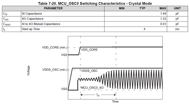
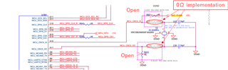
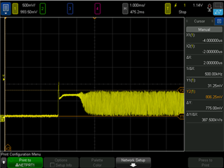
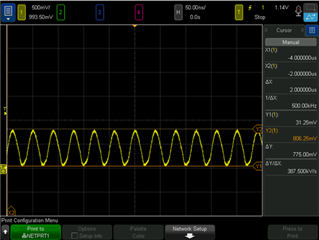
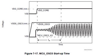
 I have a question about "Figure 7-16. MCU_OSC0 Start-up Time" from the datasheet. Here it looks like that MCU_OSC0 is only allowed to start when VDD_CORE is ramping. In reality the oscillation starts already with VDDS_OSC0, while VDD_CORE is still disabled. 

I assume that this is OK and not causing any problems?! But if this is the case, why is the Start-up Time ts shown relative to VDD_CORE stable? Shouldn't it be related to VDDS_OSC0 stable?


  • Hi Board designers, 

    Refer below inputs for the queries related to the MCU_OSC0 Start-up Time received from our device expert Paul Eaves.

    The oscillator is powered from VDDS_OSC0. So it may power-up and begin oscillation as soon as VDDS_OSC0 is applied. However, the oscillator has a few control registers which are powered by the VDD_CORE domain. So there is a chance the oscillator may not start until the VDD_CORE is valid. 

    Regards,

    Sreenivasa

  • Hi Board designers, 

    Additional inputs received from our device expert Paul Eaves.:

    The data sheet specifies the Start-up Time of MCU_OSC0, but is this a typical or maximum value?

    The value defined it the datasheet is a typical value. The max value depends on the crystal circuit components and PCB layout, so it is not possible for TI to define a maximum value. There is a good chance the start-up time will be less than 9.5ms if you select crystal circuit components that are compliant to the datasheet values and follow the recommended PCB layout.

    The waveforms were drawn to represent the worst case oscillator start-up condition to ensure reset was held long enough.


    Delay time when crystal is used

    RST1
    th(SUPPLIES_VALID - MCU_PORz)
    Hold time, MCU_PORz active (low) at Power-up
    after supplies valid (using external crystal circuit) 9500000

    In many cases you can be measuring a condition that represents the best case oscillator start-up, where it starts before the core power is available.  This is expected and does not cause any problems with respect to the processor functionality.

    Delay time when External oscillator is used

    RST2 does not include the oscillator start-up time and the timing is after the external clock is stable.

    RST2
    Hold time, MCU_PORz active (low) at Power-up
    after supplies valid and external clock stable (using
    external LVCMOS clock source)
    1200

    Regards,

    Sreenivasa

  • Hi Board designers, 

    Please refer inputs related to crystal amplitude:

    I have a question about the amplitude of MCU_OSC_XI/XO.
    Are the following points listed in the data sheet recognized as the H/L thresholds of MCU_OSC_XI/XO?

    f that is correct, looking at the waveform measurement results, it is not possible to reach the H level at Max 800mV.
    This result was the same for our boat and EVM. (The circuit configuration is also the same)
    Is this the movement you expected?


    ・Circuit configuration (EVM)

    The VIH and VIL levels defined in the datasheet only apply when sourcing the AM62Px reference clock from a LVCMOS clock source. The oscillator has an Automatic Gain Control (AGC) function that automatically adjusts the crystal circuit drive as required to maintain oscillation without over-driving the crystal. The amplitude you measured is fine for the crystal circuit implementation.

    Is there a criteria to determine that there is no problem?
    Can you give me specific spec?

    The criteria for proper device operation is selecting a crystal that meets the requirements defined in the datasheet and implementing a crystal circuit with the appropriate components that applies the correct load capacitance without exceeding the max shunt capacitance allowed by the oscillator. The oscillator will work correctly if you follow the guidelines defined in the datasheet.  TI does not expect customers to validate crystal operation by making any voltage measurements because it is very difficult to measure the voltage without the measurement equipment influencing the result. The resistive and capacitive load of voltage probes can have a significant impact on the circuit performance.

    (33) AM6442: 25MHz Crystal logic level for HFOSC - Processors forum - Processors - TI E2E support forums

    https://e2e.ti.com/support/processors-group/processors/f/processors-forum/1316040/am6442-25mhz-crystal-logic-level-for-hfosc/5002425 

    I'm trying to double check the margin leve I've got on MCU_OSC0_XI level. I've followed all recommendations and computations on CL1 & CL2.

    So according to table 7.7.3 of sprsp56f_Datasheet am6442 Sept 2022 revF.pdf , it seems that Vihmin is about 0.65 x 1.8 = 1.17V

    I've put passive probe (Cl=3.9pF), which I know may degrade a little bit the signal, to check signal level, and maximum level is about 1V => Vihmin is never reached.... but it works fine.

    I don't understand how it could work.

    I wonder if there is not something related to this sentence : 

    My assumption : in fact, due to MCU_OSC0_XI AC coupling, we just have to respect VHYS (=typ 49mV), and MCU_OSC0_XI should have a min swing of VHSYS .

    What are input level threshold on HFOSC?

    It sounds like you are trying to apply digital logic level thresholds to the HFOSC input when using a crystal circuit. The oscillator is an analog circuit. When operating with a crystal circuit the voltage across the crystal circuit is being monitored by an internal automatic gain control circuit and the amplifier gain is adjusted to maintain an oscillation amplitude that is large enough to provide a valid reference clock without over-driving the crystal. You do not need to worry with checking the amplitude as long as you selected the crystal components as described in the datasheet.

    We do not expect customers to validate margin when operating with a crystal circuit because we have already built-in enough margin as long as you follow the crystal circuit recommendations. However, it sounds like you have margin If the oscillator was able to start oscillation with the additional loading of the scope probe.

    The digital levels provided in the datasheet only apply when sourcing a reference clock from an LVCMOS clock source.

    Regards,

    Sreenivasa

  • Hi Board designers, 

    Please refer inputs related to External oscillator supply connection to take care of fail-safe operation:

    25MHz is provided from a 3.3V oscillator through a 1.8V buffer to MCU_OSC0_XI. Then I think there is no problem about the clock input at the same time with 1.8v power-up. Is it right?

    Power-Up Sequencing shows the clock starting a short time after power is applied which is typical when connecting a crystal circuit to the oscillator pins.

    MCU_OSC0 receives power from VDDS_OSC and the MCU_OSC0_XI input is not fail-safe, so the external 1.8V LVCMOS clock source connected to MCU_OSC0_XI must be the same power source that sources VDDS_OSC

    Regards,

    Sreenivasa

  • Hi Board designers, 

    Inputs related to crystal amplitude

    Do I need to set registers or use Linux commands to activate the RTC crystal(WKUP_LFOSC0) or raise the voltage level?

    A customer of mine made a board using AM625.
    In order to use the internal RTC, an external crystal oscillator is mounted, but the crystal oscillation level is ±100mV/32kHz and the voltage level is low.
    The RTC is set to Active in the figure below, but the voltage level is low.(BP_C=0, PD_C = 0)

    Could you configure the WKUP_CLKOUT0 output for 32K clock output and measure the buffered output of the clock.

    When we output the RTC clock to WKUP_CLKOUT0, it oscillates at about 3.3V and 32.768kHz.
    Is it okay to think that the voltage level of LFOSC0 is 100mV and there is no problem?

    Please refer below. 

    If the LFOSC0 output is seen on the WKUP_CLKOUT0, this should be fine.

    The WKUP_CLKOUT0 output level are based on the supply voltage connected to VDDSHV_MCU 1.8 V/3.3 V.

    Assuming the IO rail is 3.3V the measurements you are seeing looks Ok.

    Since there is no problem with the output results, we can proceed with the recognition that there is no problem with WKUP_LFOSC0=100mV

    Regards,

    Sreenivasa

  • Hi Board designers, 

    Inputs related to WKUP_CLKOUT0 

    AM62x

    WKUP_CLKOUT0 - buffered output of the MCU_HFOSC0_Xo output.

    AM62x configures WKUP_CLKOUT0 pin by default to source the HFOSC0 output (25MHz) as soon as MCU_PORz is released.

    Note: You must validate the performance of this clock output meets your system requirements in your actual system implementation. We do not define the performance of clock outputs because there are many system specific dependencies that can impact clock performance.

    The AM62x device will automatically begin sourcing the device reference clock (MCU_OSC0) to the WKUP_CLKOUT0 pin as soon as the device is released from reset (MCU_PORz 0->1). The 25M is a default output after reset and there is no software configuration required to be done.

    The output level depends on the IO supply connected to the IO supply for IO group - VDDSHV_MCU.

    The LVCMOS IOs support 1.8V or 3.3V output.

    The PPM value depends on the SOC clock source. AM62x simply connects the output of the WKUP_LFOSC0 to the WKUP_CLKOUT0 output buffer and the oscillating frequency of WKUP_LFOSC0 is completely dependent on the external crystal circuit components or LVCMOS clock source selected by the system designer. 

    WKUP_CLKOUT0 can be probed to see if it is toggling at 25MHz to indicate the processor is seeing a valid clock source during tesing, debug or manufacturing.

    My customer wants to use WKUP_CLKOUT0 for an external Wifi device.

    Taking the power-up sequence as a reference by when is it stable and ca be used?

    This IO cell associated with this pin will not be turned on until MCU_PORz has been released, reset propagates through the device, and enables the IO. This time is not defined, but it should be very soon after the rising edge of MCU_PORz.

    Note: The first clock cycle may be short or a glitch since the IO buffer is being turned on asynchronous to the clock. Any device using this clock needs to be held in reset for a few clock cycles after the IO turns on to ensure the attached device is not over-clocked by a short cycle.

    Can we get 32.768KHz on WKUP_CLKOUT0?

    If MCU_OSC0 is sourced from 25MHz reference clock:

    When HFOSC0_CLKOUT_32K_CTRL[6:0] is set to divide by 95: HFOSC0_CLKOUT_32K = [(25000000 / 95) / 8] = 32,894.7368 Hz

    When HFOSC0_CLKOUT_32K_CTRL[6:0] is set to divide by 96: HFOSC0_CLKOUT_32K = [(25000000 / 96) / 8] = 32,552.0833 Hz

    AM62A

    WKUP_CLKOUT control is the same as is in AM62x. 

    WKUP_CLKOUT0 is a buffered output of the high frequency oscillator (HFOSC0) available during power-up as default.

    You can expect the clock out on the pin during reset till the IO is configured.

    AM62P

    The AM62Px device configures the WKUP_CLKOUT0 pin to drive a low logic state when released from reset. You would need to change the clock source via CLKOUT_CTRL.wkup_clkout_sel[2:0].

    You should use the clock tree tool function in the SYSCONFIG tool to determine the clock frequencies that can be selected for this pin.

    A more accurate representation of the clock tree can be seen using the SYSCONFIG tool. This tool can be found in the AM62x product folder under Software Development Tools. You can Launch the tool from your browser then select Clock Tree when asked to select the Software Product.

    The CLKOUT0 pin can source a 50MHz or 25MHz clock. You should be able to see this configuration option in the clock tree tool. 

    Note: There is no glitch protection on this clock output when switching from one source to another, so you need to consider the potential effect of short clock pulses on the device you have connected to this pin. Some devices will not tolerate a short clock pulse. In most cases, the attached device will allow clock glitches while it is being held in reset. If so, you could use a GPIO with an appropriate external pull to hold the attached device in reset until the appropriate clock source has been selected and the clock is stable. Once the clock is stable, the GPIO can be driven to release the attached device from reset.

    Regards,

    Sreenivasa