This thread has been locked.

If you have a related question, please click the "Ask a related question" button in the top right corner. The newly created question will be automatically linked to this question.

[FAQ] AM625 / AM623 / AM620-Q1 / AM62Ax / AM62Px / AM62D-Q1 / AM62L / AM64x / AM243x Design Recommendations / Custom board hardware design - Drive Strength Configuration for dual-voltage LVCMOS and SDIO IO buffers and fixed 1.8V 1P8-LVCMOS, buffers

Part Number: AM625
Other Parts Discussed in Thread: AM62A7, , AM62L, AM62P, AM6422

Tool/software:

Hi TI Experts,

I have the below query

AM62A7: How can we change the drive strength of the SPI interface
AM625: How to change the drive strength of the ethernet interface IOs
AM625: How to change the drive strength of the OSPI interface IOs

In general can i configure the drive strength for the SOC IOs or peripherals.

  • Hi Board designers, 


    We do not currently support changing the drive strength.

    We only support the default drive strength currently, and customer should use the device IBIS models to understand the actual output buffer drive strength.

     Drive Strength Configuration:

    TI currently does not support configuring any other drive strength besides the nominal (default) value for SDIO and LVCMOS buffers, as the nominal value is the only configuration at which chip-level STA (Static Timing Analysis) is closed. The nominal value corresponds to a 40Ω for SDIO and 60Ω for LVCMOS. The IBIS model has been updated to contain only drive strengths where the timing is closed internally.

    The drive strength must remain in the default state since this is the only condition used during timing closure of the peripherals.

    The SOC has been currently configured for proper operation when using the default drive strength.
    Changing the drive strength may cause functional issues. Therefore, we currently do not support changing drive strengths.

    Regards,

    Sreenivasa

  • Hi TI Experts,

    Do you have plans to support other drive strengths other than the default drive strength?

  • Hi Board designers, 

    We do not currently support changing the drive strength.

    We have received similar requests. The Systems/Design team is reviewing, analyzing the requests and performing internal simulations.

    We are internally performing simulation and tests to support drive strength configuration for the LVCMOS IO.

    We are planning to support NOM (currently configured) and FAST drive strength for LVCMOS IOs.

    I have no additional inputs or timeline for inputs. I will update the FAQ when i hear from the team.

    Last Updated: 30th August 2025

    Regards,

    Sreenivasa


  • Hi Board designers, 

    Additional inputs:

    (43) AM625 / AM623 / AM62A / AM62P / AM62D-Q1 / AM64x / AM243x hardware design - I/O Drive Strength Configuration for SDIO and LVCMOS - Processors forum - Processors - TI E2E support forums

    • the PCB track must be 40 Ohm to match the driver/receiver impedances of SDIO MMC1 (CLK + DAT0-3 + CMD)

     Customer needs to consider the impact of trace impedance on their entire system implementation.  This not something TI can answer.  For example: 40 ohms may be a better match for the AM64X output impedance, but it may not be the best match for the attached device.  In reality, it may be better to split the difference and target a trace impedance of 45 ohms if the attached device has a 50 ohm source impedance.  This is why customer should be performing simulations to validate signal quality on their specific system implementation.

    Slew rate control and source impedance are two different things.  We do not provide slew rate control on the IOs implemented in AM64x.  The device is trimmed during final test to target a fixed source impedance as defined in the IBIS model.  All peripherals were timing closed based on the source impedance defined in the IBIS model.  This should be 40 ohms for the IOs associated with MMC1

    Regards,

    Sreenivasa

  • Hi Board designers, 

    Inputs related to drive strength for AM62L

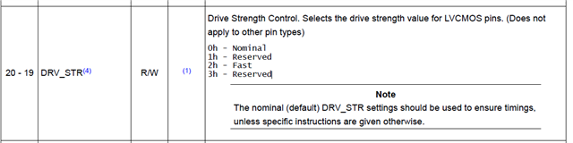
    Please refer below table of the processor-specific TRM for information related to drive strength (Dual-voltage IOs, For LVCMOS Buffer Type Only) or slew rate (Fixed-voltage IOs, For 1P8-LVCMOS Buffer Type Only) configuration supported:

    Pad Configuration Registers
    Pad Configuration Register Functional Description
    The pad configuration registers are used to configure most of the device pads. Each pad configuration register is
    associated only with one pad and has bits as described in Table 14-3860.
     Description Of The Pad Configuration Register Bits for AM62L IO pad configuration:

    Nominal impedance

    Dual-voltage IO buffers 

    SDIO Buffer - 40Ω

    LVCMOS Buffer NOM- 60Ω

    LVCMOS Buffer FAST - 50 Ω

    The above is valid for AM62x, AM62A, AM62P, AM64x, AM243x

    Fixed voltage 1.8V IO buffers (AM62L):

    1P8-LVCMOS Buffer – 50 Ω

    AM62A

    (4) Use of settings other than the reset value could invalidate datasheet timings.

    Note:

    The IO buffer output impedance is valid when the IOs are operating (operating voltage) at 1.8V or 3.3V
    The IO buffer output impedance is valid when the IOs are operating withing the ROC as per the processor-specific data sheet for a given operating voltage.

    Note:

    We are working to enable a faster drive strength option, but there is no plan to support a reduced drive strength mode. 

    timeframe or ETA for the faster drive strength feature

    I do not, it is currently down to alignment for an SDK release to contain the feature as this has to be supported and enabled in SW. 

    Regards,

    Sreenivasa

  • Hi Board designers, 

    Inputs related to verifying drive strength change:

    Customer is measuring signal rise/fall time as a way to confirm drive strength changes.

    The drive strength register changes the output buffer source impedance, which may not have a significant impact on signal rise/fall time at the far end of the PCB trace. The bandwidth of the PCB trace can also limit the signal rise/fall times. The reflections that occur on the PCB trace can distort the signal shape. In some cases, these reflections may result in waveform shapes that are counter-intuitive or unexpected. 

    They may be able to observe a waveform shape difference at the source end of the signal trace that can be used to confirm the output impedance change if the PCB trace is long enough for the signal to rise before the first reflection from the far end of the PCB trace returns.

    We designed in our PHY and AM64 at our customer.

    The latest assessment shows that there might be some issues with our spec: 

    We were taking some measurements on our board where we use the AM6422 and DP83822 PHYs and I noticed some values that I was wondering if you could help me clarify.

     In the AM6422 Datasheet I see the information below:

    Looking at our PHY:

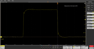
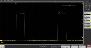
    I attached a sample measured of RX_D1 and TX_D1 as references, but similar timings are observed on all relevant signals:

    As you can see above, when it comes to the TX signals the requirements are fulfilled both for the processor and the PHY.

    This is, unfortunately not the case for the Receive signals, so my questions are :

    1. Why is this requirement from the processor so restrictive?
    2. Would this timing from the RX line cause an issue with the processor?(lost frames etc.)
    3. Could this be somehow be adjusted by the processor or the PHY?(Driver strengths or timing parameters)

    The minimum input slew rate defined for AM64x is equivalent to the input rise/fall time requirements defined for the PHY. A 20% to 80% or 80% to 20% voltage change is a voltage change that is equal to 60% of VDD. In your case, VDD is 3.3V and 60% of 3.3V is 1.98V. Changing the signal by 1.98V in 0.75ns gives a slew rate of 1.98V/0.75ns = 2.64V/ns. So, the requirements are the same for both devices and matches the signal rise/fall times defined in the RGMII standard.

    Measuring the rise/fall time at the source end of an LVCMOS signal can be misleading. The voltage at the source end of the signal only steps up to a mid-supply potential until the signal has time to propagate down to the far end of the signal trace and the high impedance connection at the far end returns an in-phase reflection to the source. Therefore, measuring a 20/80 rise/fall time at the source will include 2x the PCB trace propagation delay in your measurement. The far end of the signal trace doesn't see this additional delay. I suggest you find a place to probe the RX_D1 signal near the AM64x device to get an accurate rise/fall time measurement for the RX input. Otherwise, you could subtract about 0.334ns for each inch of signal trace from the measured value at the source to get a value that is close to what is seen by the RX input. For example, you would subtract 1ns from the 1.7ns fall time measurement if you have 3 inches of PCB trace between the probe point and the RX input pin.

    (+) AM62P-Q1: drive strength of EMMC I/F - Processors forum - Processors - TI E2E support forums

    The SDIO and LVCMOS references from the other E2E thread was with respect to these specific IO buffer types. The IO buffer type for each device pin can be found in the BUFFER TYPE column of the Pin Attributes table in the device datasheet. The AM62Px MMC0 port uses the "eMMCPHY" buffer type rather than the SDIO buffer type. The output buffer associated with the eMMCPHY buffer type supports multiple source impedances, where it can be configured to operate with a source impedance of 33, 40, 50, or 66 ohms. However, I'm not sure if we plan to support all of these options. I'm fairly sure 50 ohms will be supported and there is a good chance 40 ohms will be supported. I will need to check and get back to you on this topic.

    You are able to control the output source impedance of the AM62Px MMC0 port via the DR_TY bit field of the MMC_SSCFG_PHY_CTRL_1_REG register.

    I have discussed the source impedance options with our design team, and they said customers should attempt to design their PCB to operate with the 50 ohms source impedance option since this is the recommended value defined in the eMMC standard.

    Regards,

    Sreenivasa