


Other Parts Discussed in Thread: SYSCONFIG
Hi Expert
We have some problems in designing our products and would like to help.Could give us a reference design to satisfaction below request ?
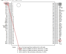
Background: Our machine is based on the DESIGN of AM3358(324PIN), because we need to start the machine faster, so we choose the NorFlash chip design.
Prerequisites:
1. DDR3L (MT41K256M16HA-125)
2. RMII1(100m Network)
3. LCD(RGB-480*800)
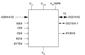
4. NorFlash (MT28EW256ABA),256Mbit
5. NandFlash(MT29F8G08ABAB), 8Gbit (or larger)
6. The TF card
I refer to TRM manual 7.1.2
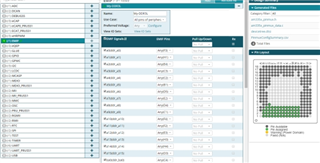
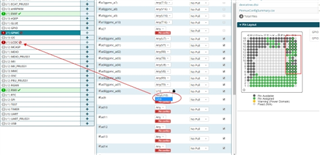
I have carried out pin configuration in TI PinMux Tool and found that the conditions cannot be met. It may be that some parts are not properly configured. I hope to obtain your technical support.
My configuration is as follows:
1. DDR3L
2. RMII1(100m Network)
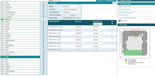
3. LCD(RGB-480*800)
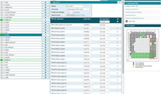
NorFlash(MT28EW256ABA)256Mbit, address line has 24, data line has 16 and control line, considering the sharing of data line + asynchronous or synchronous mode are not able to go on, occupy the LCD pin, do not know how to deal with, hope to get a help.
I have seen the design of tmdxice3359_sch_3h0013_v2_1a about NOR Flash (16 Mbit) on the official website, but it cannot meet the design of 256Mbit. Can you provide a reference design for designing NAND Flash&NOR Flash together? (or help to configure TI PinMux Tool, provide a reference).
Consultation the second option:
A. DDR3L (MT41K256M16HA-125)
B. RMII1(100 MBIT Network)
C. LCD(RGB-480*800)
D. NorFlash (MT28EW256ABA),256Mbit
E. eMMC (MTFC8GAMALBH), 8 gb
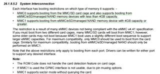
I noted in the TRM manual that MMC1 has a chance to be larger than 4Gb; The MMC0 limit is 4Gb.
Is it feasible? Reserve MMC1 channels for eMMC. Is there a reference design for that? (or provide a TI PinMux Tool configuration file)

