This thread has been locked.

If you have a related question, please click the "Ask a related question" button in the top right corner. The newly created question will be automatically linked to this question.

[FAQ] AM625 / AM623 / AM62A / AM62P / AM64x / AM243x Design Recommendations / Custom board hardware design – POK VMON Voltage Monitor

Part Number: AM625
Other Parts Discussed in Thread: AM623, AM6546, AM6442, AM2432, TDA4VH-Q1, TDA4VH

Tool/software:

HI TI experts,

I have queries related to the voltage monitoring capability of the SOC POK module types, accuracy., design recommendations and supported rails.

  • HI Board designers, 

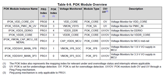
    Refer below description of POK Modules.

    Power OK (POK) Modules

    POK modules are responsible for accurately detecting the voltage levels. Each module is trimmed to account
    for process and temperature variations.

    Two types of POK modules are implemented in this family of devices - POK and POK_SA. See Table 6-9 about
    the type of a POK and the voltage it is monitoring.

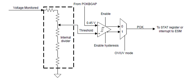
    POK Block Diagram

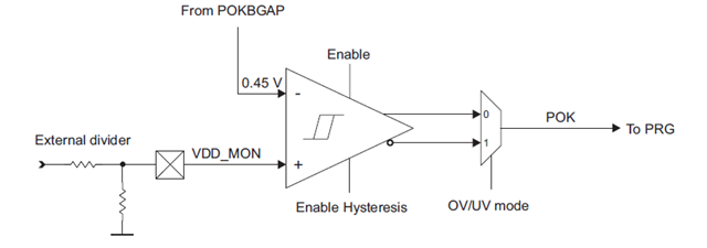
    POK_SA Block Diagram

    Regards,

    Sreenivasa

  • HI Board designers, 

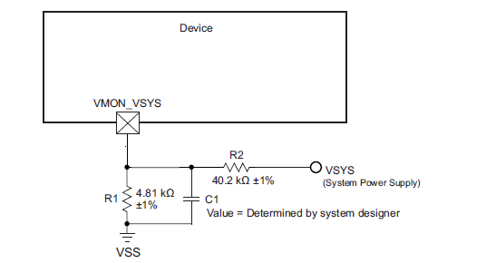
    Refer below guidelines for implementation of VMON_VSYS voltage divider 

    System Power Supply Monitor Design Guidelines

    Recommend implementing the voltage monitoring functionality using VMON_VSYS for early detection of supply failure. It is meant to be a power-fail indicator for the main input (higher) voltage rail that enters the PCB. For example, 5, 12, or 24 volts.
    The error associated with this monitor would require you to set the threshold significantly lower than the nominal to avoid false trigger
    Refer System Power Supply Monitor Design Guidelines section of the processor specific data sheet

    System Supply Monitor Voltage Divider Circuit

    Q. When we check the description in the data sheet, it states that if the VMON_VSYS pin drops below 0.45V, a power fail event will be triggered. What happens when this trigger occurs?

    When the voltage applied to VMON_VSYS  drops below the internal reference voltage, it triggers an interrupt that is routes to the ESM.  Handling post ESM interrupt is configured by software and can range from interrupting a core to resetting a device.

    Regards,

    Sreenivasa

  • HI Board designers, 

    Refer below guidelines for monitoring CAP_VDDS_MCU

    Use case: 

    We wanted to adjust the voltage range for the CAP_VDDS_MCU monitor.
    According to TRM we selected the following TRIM values for
    POK_VMON_CAP_MCU_GENERAL_UV = 2Eh = 0101110b = 1.728V
    POK_VMON_CAP_MCU_GENERAL_OV = 22h = 0100010b = 1.888V
    We get UV interrupts with these settings, although the IO supply is correct.
    The default values seem to be (we read the register before writing it):
    POK_VMON_CAP_MCU_GENERAL_UV = 23h = 0100011b = 1.502V
    POK_VMON_CAP_MCU_GENERAL_OV = 1Dh = 00111101b = 1,781V

    Okay, now I think I know what is going on. It looks to me like they think this VMON is monitoring a 1.8V supply, but in reality this VMON is tied to CAP_VDDS_MCU and doesn’t monitor for 1.8V threshold.

    It is not a fixed voltage. When the respective VDDSHV is operating at 1.8V, the pin should have the same potential as the VDDSHV source. When the respective VDDSHV is operating at 3.3V, it should have a potential that track to ½ of the VDDSHV source.

    We did not publish the voltage on these pins in the datasheet because we never expected anything to be connected to them. I only recently learned one of the LDO outputs has an internal connection to a POK input.

    When VDDSHV is ramping to 3.3V the LDO output will track VDDSHV until it gets up to about 2.4V. This is when bias supply circuit changes from what I call switch mode to LDO mode. At this point it begin to track ½ VDDSHV. I suspect the output capacitance will hold the 2.4V potential for a period of time before the IO bias circuits draw enough current to discharge the capacitor back down to the ½ VDDSHV potential.

    I would expect a similar thing to happen as the VDDSHV decays. When VDDSHV drops below 2.4V the bias supply circuit will switch back to switch mode, where the potential of VDDSHV is applied to the capacitor.

    I do not think this will be a problem for the POK configuration since it will only be configured after the IO power is stable. This is mostly a concern for selecting the capacitor with an appropriate voltage rating. This is why we updated to signal description note to include the capacitor voltage rating.

    Regards,

    Sreenivasa

  • HI Board designers, 

    Refer below guidelines for VMON threshold accuracy 

    The band-gap reference alone can have up to +/-3% of error. 

    There may be other errors that need to be considered in addition to the band-gap.  Things like internal resistor divider matching and the error introduced by POK input leakage through the voltage divider. This could add-up to an additional 1%

    This accuracy is valid for POK and POK_SA

    Regards,

    Sreenivasa

  • HI Board designers, 

    Refer below guidelines for POK threshold setting 

    Threshold setting use case 

    Q. IPOK_VDDSHV_MAIN_3P3  UV limit is per default 3.015V but recommended min value according data sheet is 3.135V.  The voltage could be below ROC and still the POK would not detect it.
    The same is true for VMON_1P8_SOC and VDDR_CORE and all of them have no power architecture dependencies (are fixed by design).

    This isn’t a mistake the POK are defaulting wider than recommended operating conditions because this is the recommendation in the

    POK spec – to leave tolerance for POK component variation

     3% total tolerance for POK accuracy + 1% guardband is what the spec has.

    Customer can pull this in if they want but they need to then make their power supply is tighter or risk false triggers.

    Regards,

    Sreenivasa

  • HI Board designers, 

    Recommendations on CAP_VDDSx value 

    The LDO specification is 0.8uF to 1.5uF.  The capacitor should be within this range, considering bias, degradation over time etc.

     Q. With a 6.3V/10V, X7R cap selected, considering the DC effect and other degradation, the cap value could go down to 0.7 uF.  Higher cap value may call for using a 0402 cap and that could have an effect on the layout.

    Does the capacitance depend on number of IOs used for the specific IO supply rail and the IOs current source/sink  or irrespective of the IO usage, the capacitance is required.

    https://www.kyocera-avx.com/docs/techinfo/CeramicCapacitors/mlcc-dc-bias-characteristics.pdf

    https://community.infineon.com/t5/Knowledge-Base-Articles/DC-Bias-characteristics-of-Multilayer-Ceramic-Capacitor-MLCC/ta-p/250035#.

    The cap value is independent of IO count and activity. It is required for stability of the LDO to generate BIAS supply. Any value beyond this specified range could make BIAS generator unstable resulting in over voltage stress.

    Additional Guidelines 

    Select cap with less the 1 ohm ESR
    Ensure the PCB loop inductance is < 2.5 nH
    Select 0201 package 
    Refer SoC Data sheet

    Regards,

    Sreenivasa

  • HI Board designers, 

    Links to E2Es and additional information added below:

    AM623: dying gasp
    e2e.ti.com/.../4995264

    SYS-MON UV Interrupt Event on R5F
    e2e.ti.com/.../4045303

    voltage details for CAP_VDDS and CAP_VDDS0_MCU pins
    e2e.ti.com/.../dra829v-voltage-details-for-cap_vdds-and-cap_vdds0_mcu-pins

    What is the hysteresis window of POK comparator?
    e2e.ti.com/.../4689435
    POK support in Linux?

    e2e.ti.com/.../am625-pok-support-in-linux
    There is no software requirement for Linux to support POK.
    POK, as you mentioned, is supported in the safety SDL package, I believe.
    I found the POK section in latest MCU+ SDK SDL. Still functionality is not really clear as I am missing examples that would trigger some action or so.
    Recommended POK threshold

    e2e.ti.com/.../4793549
    the POKs circuits are setup to monitor the average voltage of a domain. As such, they will not catch a single instantaneous dip in the voltage; a bad POK value indicates something is wrong while a good POK value does NOT indicate that nothing is wrong.
    Given the behavior of the POKs, I would tend to treat them as sanity checks, and because of that, I would leave margin in the thresholds.
    For the CAP_VDDS, I think you will find that for 1.8V I/O rails, the CAP_VDDS voltage will be 1.8V; for 3.3V I/O rails, the CAP_VDDS voltage will be 3.3V / 2.
    The POK measures the voltage at n time slots (defined by DEGLITCH_SEL). The voltage must be out of range for all time slots before the POK is delared BAD. The POK is NOT an instantaneous monitor but instead is looking at the long term behavior of the rails.
    The +/-5% quoted from the data manual really is an instantaneous voltage requirement.
    The customer is expert on how they use this block in their safety concept. They can set the voltage threshold as they see fit with due precautions for false failures.

    AM6546: WKUP_POK9 (MAIN/SoC 1.8V)
    e2e.ti.com/.../4486085

    AM6442: Power OK module behavior at UV detection
    e2e.ti.com/.../4172846

    AM2432: Power Up Sequencing
    e2e.ti.com/.../am2432-power-up-sequencing
    VMON_VSYS, VMON_1P8_MCU, VMON_1P8_SOC, VMON_3P3_MCU, and VMON_3P3_SOC cannot be directly used to cause a reset. If the customer needs to generate a reset based on one of these signals, they will need to leverage the Error Signaling Module (ESM).

    AM6442: How to use the POK modules
    e2e.ti.com/.../3945472

    AM6442: How to use the VMON_VSYS pin
    e2e.ti.com/.../3932658

    e2e.ti.com/.../4027705

    what is the worst case voltage offset expected between the power pins of the device and the on-die voltage monitoring on VDD_CPU and VDD_CORE?
    The offset voltage is negligible.

    Can you clarify if POK monitor can only alert ASAR about abnormal power supply behaviors or also can protect some subsystems from running in unsafe way?
    POK monitor is an ASIL or QM feature?
    The Internal POK monitor is a diagnostic that monitors voltages for undervoltage (UV) or overvoltage (OV) conditions and is a safety feature considered
    as part of the FMEDA. The internal POK monitor will provide notice of detected faults to the ASAR core or safety checkers running on the MCU Channel M4F.
    The Internal POK monitor, by itself, is not able to take any active measures to shut off the power source. Such a feature is typically accomplished
    via an external PMIC after having received notice of a fault (through ESM signaling of a fault pin or over an itnerface such as I2C by software responding
    to an interrupt received from the POK).

    VMON_3P3_SOC
    do not have a 3.3V rail to park this signal. If my input voltage to the module is at its lowest point (3.135V),
    the actual 3.3V will be slightly lower (depending on the losses in the chain). Therefore, I need to know how the SoC reacts.
    What exact threshold values (including hysteresis) trigger the monitor feature? Is it possible to turn off the reaction?

    Tying the unused VMON_3P3_SOC to ground is the recommended solution when no 3.3V rail is available and the customer does not want to use this POK function.
    This is not true for the VMON_1P8 circuitry, where grounding this signal would short internal 1v8 supplies.


    TDA4VH-Q1: VSYS_3V3 and VDD_CPU_AVS monitor
    In the reference design, VSYS_3V3 and VDD_CPU_AVS are connected to VMON of SoC. I would like to know it is a must or an option? Given that VSYS_3V3 and VDD_CPU_AVS have been monitored by the PMIC, do we have special reason for monitoring them by different device?
    The CPU voltage should be connected to dedicated monitor, but the other monitors are optional and can be assigned based on the customer's voltage monitoring requirements.
    Could you tell me how to understand the functional difference between PMIC monitor and SoC VMON (POK module)?
    The SoC VMON can simply generate an interrupt to the processor, and then software decides how to handle.
    PMIC monitors can function similarly, but also have option to take direct action (like initiate power down) without software interaction (if setup accordingly).


    TDA4VH-Q1: Full Efuse peripheral and register list

    As I've been going through all the TDA4VH documentation, I have found it difficult to find a clear list of all peripherals/blocks that correlate to efuse registers. Additionally, it is not clear which registers in the register spreadsheet are efuse registers.
    As a part of our process, we would like TI to provide a comprehensive list of peripheral/blocks and relative efuse registers, such as for VTM, POST, POK, etc., in order for Ford to assess what the settings will be in production and to determine if we require any changes, for which we would need to make requests to TI.
    Can someone please provide this list? Initially, I was working with Suman Anna (s-anna@ti.com), but I was not able to find him and tag him in this post.

    Discussed the following with the hw apps and silicon program management team. We can discuss further upon your return.
    The eFuse parameterization of the TDA4VH device is TI Internal information - the exact configuration is tied to specific part numbers and to TI’s validation of functionality relevant to these specific part numbers.
    TI does not support any eFuse parametrization with customers (ie TI does not blow efuses on a customer’s behalf): There is no process in place for such customization; as such, there is no part number schema that can accommodate custom PN. FWIW, there is a valuable benefit to Ford: continuity of supply.
    For POST override configuration, the production setting will be “override disabled”: the end system selectively enables/disables POST via the MCU Bootmode pins.

    Protection against voltage and clock glitches attacks
    What type of protection does the TDA4 have against voltage and clock glitches from an outside source/attacker?
    The attack is trying to force the TDA4 to operate outside of its expected conditions, allowing unexpected behavior.
    From the Security angle. The attack I have in mind is similar to CVE-2019-17391.
    An attacker using fault injection, a clock and\or voltage glitches, could gain access or corrupt the eFuse/OTP keys,
    while the keys are read out of memory after a reset. An attacker could corrupt the keys enough times to be able to reverse engineer the keys.
    We have no inherent protection in design for these attacks.
    HW Safety monitors [POK (Power OK), VTM (Voltage / Temp Monitor) and DCC (Dual Clock Comparator)] could be used to detect such attacks and trigger reset.

    I am duplicating my response to that thread here for completeness
    TDA4x devices do not have explicit HW to prevent clock/voltage glitch attacks at initial boot.
    TDA4x device to have safety checkers that can be setup after boot to detect such attacks.
    These consist of: POK (Power OK), VTM (Voltage / Temp Monitor) and DCC (Dual Clock Comparator).

    Other mitigations
    eFuse key data is autoloaded to registers at startup and includes error correction eFuses data that ROM applies to correct read errors.
    If there are any read errors in key data, then boot authentication will fail.
    Note - Extraction of the Public Key in eFuse, by definition, is not a vulnerability
    Extraction of the Symmetric Key is a vulnerability only if optional encrypted boot is used.
    But, system firewalls configured to prevent access to the secure registers where the secure eFuse data is read into.
    Only the TI Security firmware (TIFS) will have access to these registers.

    why AM263x do not implement Brown-out Reset (BOR) circuit like C2000 MCU. I am also a little confused on this
    AM263 was designed with the expectation that an external voltage supervisor would be used to monitor all the power rails and issue a POR externally if the rails drop.

    POK hysteresis
    14.2.1.1.1.528 CFG0_POK_VDDSHV_MAIN_1P8_UV_CTRL Registers
    14.2.1.1.1.529 CFG0_POK_VDDSHV_MAIN_1P8_OV_CTRL Registers
    14.2.1.1.1.530 CFG0_POK_VDDSHV_MAIN_3P3_UV_CTRL Registers
    14.2.1.1.1.531 CFG0_POK_VDDSHV_MAIN_3P3_OV_CTRL Registers

    Regards,

    Sreenivasa

  • HI Board designers, 

    Handling of unused VMON_VSYS 

    refer to Connectivity Requirements section of the data sheet

    The extract is provided below

    Regards,

    Sreenivasa

  • HI Board designers,

    VMON_VSYS pin monitoring in Software

    Is software able to read back the voltage detected on the VMON_VSYS pin?

    We are feeding the VMON_VSYS pin with a 5V rail in our current design and would like to read back the voltage sense.

    The Power monitoring is documented in the TRM Chapter 5.2.2.1.1 "Power OK (POK) Modules".

    POK is not used in Linux, so I am routing your query to our hardware expert for details.

    We are feeding the VMON_VSYS pin with a 5V rail in our current design and would like to read back the voltage sense.
    Please note that this is a comparator output.
    That would mean we would either read back 0 or 1 on the output then from the Sitara? Correct.

    Regards,
    Sreenivasa