This thread has been locked.

If you have a related question, please click the "Ask a related question" button in the top right corner. The newly created question will be automatically linked to this question.

[FAQ] AM623: MMC0 HS200 slew rate

Part Number: AM623

Tool/software:

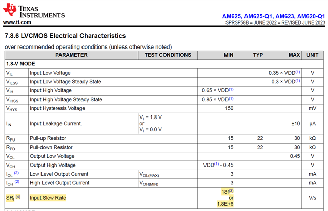
#1. Did not find MMC0 HS200 slew rate data in datasheet timing section, so section 7.8.6 LVCMOS Electrical Characteristics data applies?

#2. The Min vale: 18f or 1.8E+6, the two value are quite different, 18f=18x200MHz, 1.8E+6=1.8M for HS200, which is the right one for HS200?

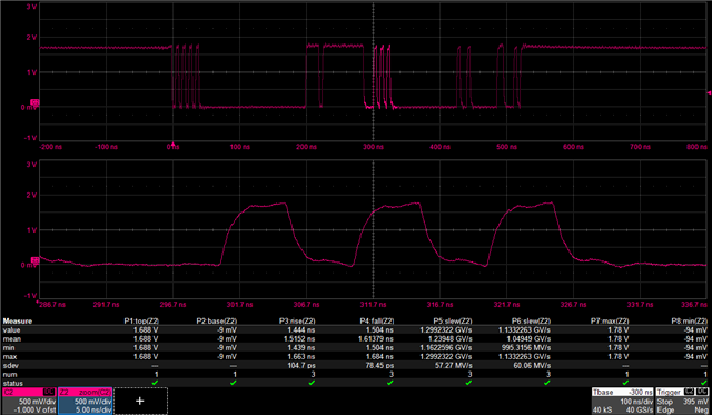
#3. On custom board, the slew rate of read data with eMMC is about 1V/ns, see below picture, P5 and P6 for rising and falling edge slew rate, Is it acceptable for AM62x at HS200?

#4. How is the slew rate requirements specified? What impaction if lower slew rate signal?

  • 1) We only define Input slew rate for modes which have specific or fixed input timing requirements. The clock output to data capture time relationship is not fixed for the HS200 read data path since this mode requires data training. The data training algorithm used a known data pattern to select a data capture time that is centered in the data valid window. There is no specific input slew requirement since tuning searches across an entire bit time to find the center of the data valid window. However, the width of the data valid window is a function of input slew. The signal transition needs to be fast enough to provide a reasonable data valid window for the data training algorithm.

    2) It is very important to limit the amount of time the applied signal spends within the voltage region between VIHSS and VILSS. The minimum input slew rate limits are required to ensure long-term reliability of the input buffer. 

    The minimum slew of 1.8E+6V/s (1000ns when operating at 1.8V) is not a function of toggle frequency and it represents the slowest signal that can be applied to the AM62x input buffer. The minimum slew of 18fV/s (0.5ns when operating at 1.8V with a 200MHz toggle) is a function of toggle frequency and represents the minimum slew rate allowed for a specific operating frequency. The limit of 18fV/s is the more restrictive of the two limits, so this is the requirement to ensure long-term device reliability. In some cases, a specific peripheral may have a more restrictive requirement to ensure timing. 

    3) I would not expect an HS200 timing issue for read data with this signal slew, but it appears to violate the 18fV/s requirement. 

    4) Input slew rate can impact long-term device reliability and input timing.

    Regards,
    Paul

  • Hi Paul,

    Thanks, per customer's feedback I read upper again especially for #2. I split it to be better understanding for me.

    #1. 1.8E+6V/s is the slowest signal that can be applied to the AM62x input buffer

    [TT] 1.8E+6V/s=1.8V/1000ns

    #2. 18fV/s (0.5ns when operating at 1.8V with a 200MHz toggle) is a function of toggle frequency and represents the minimum slew rate allowed for a specific operating frequency

    [TT] 18fV/s=18x200MV/s=18*200/1000ns=3.6V/ns

    so this is the requirement to ensure long-term device reliability

    #3. Which one is required to ensure long-term reliability?

     3.6V/ns is hard to meet. even HS400 eMMC device only require Slew Rate>1.125V/ns. 

    Does AM62-SK board achieved the requirements?

    Input slew rate can impact long-term device reliability and input timing.

    #4. Customer would like to how it impact long-term reliability as they can't achieve the requirement, the SR=0.92V/ns on their board, need guide to quantify the impact and evaluate the risk?

  • Let me review how we derived the frequency dependent limit found in the datasheet to make sure I didn't make an error.

    Lets assume the limit is correct for now.

    As mentioned in my previous reply, the limit of 18fV/s becomes the more restrictive in this case. See Note 5 associated with the Input Slew Rate parameter, SRI. The note defines which value applies by saying "Select the MIN parameter which results in the largest value".

    The non-frequency dependent limit of 1.8E+6V/s becomes the larger value when the signal toggle rate is less than 100kHz. 

    The frequency dependent limit of 18fV/s becomes the larger value when the signal toggle rates is greater than 100kHz.

    We basically need to limit the amount of time the input buffer is exposed to a mid-supply potential. The concern is related to electromigration in the input buffer caused by shoot-through current that flows from VDD through the input buffer to VSS as the signal transitions through the mid-supply region. The slew rate limits ensure the device is not exposed to this condition for too long over the life of the product.

    The risk associated with violating the limit is the possibility of the input buffer failing before the device POH limit.

    Regards,
    Paul

  • Hi Paul,

    understood the theory now, and know it will reduce POH although may not impact functionality. 

    But it is hard to achieve the SR requirement on board, so customer wants to evaluate how long will be reduced with SR=0.92V/ns VS 3.6V/S which can work 100K hours POH, 10%, 20%, 50%?

    If AM62-SK eMMC signal meets the requirements, we can say customer should optimize their layout. 

    I know there would be many factors to impact the POH together, but how to feedback to such a question?  

  • I will need to schedule a meeting with the IO designer and our reliability team to discuss this topic. It may take a few days before I have any additional information.

    Regards,
    Paul

  • Hi Paul,

    Is there feedback?

  • We performed some additional reliability analysis and determined the formula of 18fV/s is more aggressive than necessary at higher-frequency toggle rates. We determined the slew rate of 1.125V/ns defined in the eMMC standard for HS400 mode is acceptable for peripheral signals toggling at rates that approach 200MHz. The formula in the datasheet will most likely be changed, or an additional formula added to reflect a relaxation for higher-frequency toggle rates, where the current formula may remain the same for lower-frequency toggle rates. We are still discussing how to present the updated slew rate requirements in the datasheet.

    Your customer should try to reduce PCB loading such that the attached eMMC device is able to achieve an input slew rate of 1.125V/ns. 

    Regards,
    Paul

  • Hi Paul,

    As data line signal switch rate doesn't like eMMC_CLK which switch each cycle, from IO POH perspective, can lower down data line slew rate than eMMC_CLK? if eMMC_CLK slew rate require 1.125V/ns, can eMMC data line accept 50% of eMMC_CLK slew rate if assume eMMC data line switch rate is 50%?

  • The reliability analysis was performed on the worst-case operating condition, where CLK was constantly toggling for the life of the device. I do not think we have reliability data that represents the reduced toggle rate of the data signal. It is going to be difficult to find resources to perform this analysis and is likely to take a long time before we get results. Therefore, I'm not able to comment on the availability of an answer to this question. I would need to discuss this topic with the IO designer.

    Regards,
    Paul

  • I should have asked, how were they able to achieve the improved slew rate on CLK?

    I would have expected any PCB board layout improvements that result in a better slew rate on CLK would also be seen on the DAT/CMD signals.

    Regards,
    Paul

  • There isn't serial resistor on CLK, so the rising edge is much sharp can meet slew rate requirement.

    If replace 22/33ohm serial resistors on DAT/CMD with 0ohm, the slew rate can also meet requirement, but some boards may trigger IO/CRC/CQE error, with 22/33ohm resistor can eliminate the error from test result, but can't meet slew rate. 

    Customer said other competitor's devices don't have such strict slew rate requirement.

  • We only care about the signal slew rate that is applied to an enabled AM62x input buffer.

    The slew rate is not a concern for CLK signal as long as they turn off the associated input buffer with the respective RXACTIVE bit. This will not be possible for the IOs associated with the DAT/CMD signals since they are bidirectional. The external series resistor should provide some isolation from the load when AM62x is driving DAT/CMD, which should allow the signal to have a faster slew rate at the AM62x pin. We are only concerned with the signal slew rate on the AM62x pin since that is what is sourcing the AM62x input buffer. The external series resistor should not have a big impact on the signal slew rate at the AM62x pin when the attached device is driving DAT/CMD.

    They need to be measuring the signal slew rate of the AM62x pin. Where are they measuring the signal slew rate?

    Regards,
    Paul

  • We only care about the signal slew rate that is applied to an enabled AM62x input buffer.

    ooh, AM62x eMMC_CLK is not mentioned to be used as a retiming input like that of AM335x. I assumed they are similar.

    Where are they measuring the signal slew rate?

    Closed to AM62x side as possible.

  • The eMMC clock in AM62x is not looped back for retiming. AM335x did not have internal delay lines that could be used to optimize timing, so the clock was looped back at the pad to help compensate for the some of the delay inserted in the roundtrip time associated with read operations. It would not be possible to close timing for the faster data transfer rates supported in AM62x without having the internal delay lines. You do not need to loopback the clock once you have internal delay lines to compensate for external delays.

    When you say they are measuring slew rate close to AM62x, are they probing on the actual device pin.  If not, the measured slew rate will not be the same that is seen by the AM62x input buffer. For example, the measured slew rate will have a 100ps mid-supply step include in the slew rate measurement if they probe the signal 0.3 inches from the AM62x pin. The mid-supply step gets shorter as you probe closer to the AM62x pin and gets longer as you probe further from the AM62x pin. The slew rate measurement is only accurate when probing the signal at the AM62x pin.

    You mention competitor devices do not have similar slew rate requirements. This may be the case if these devices were implemented in a less-advanced process node, where the circuit geometries are larger. It may also be possible that competitors do not understand the risk associated with an input speeding too much time in the mid-supply region.

    Regards,
    Paul

  • The mid-supply step gets shorter as you probe closer to the AM62x pin and gets longer as you probe further from the AM62x pin.

    Is the conclusion for a pin in output state?

  • The reliability analysis was performed on the worst-case operating condition, where CLK was constantly toggling for the life of the device. I do not think we have reliability data that represents the reduced toggle rate of the data signal. It is going to be difficult to find resources to perform this analysis and is likely to take a long time before we get results. Therefore, I'm not able to comment on the availability of an answer to this question. I would need to discuss this topic with the IO designer.

    Since reliability analysis based on worst-case, the IO buffer wear is accumulation result, then we can deduce in real case, it is acceptable to lower the slew rate, waiting for your discussion conclusion.

  • The mid-supply step will be equal to 2 times the PCB trace delay at the output buffer. The mid-supply step will be equal to zero at the input buffer connected to the far end of the PCB signal trace. The mid-supply step decreases from 2 times the PCB trace delay to zero as you move the probe from the source to the end of the PCB signal trace. The mid-supply step will persist for the time it takes the signal to propagate past the probe to the end of the PCB trace and return back to the probe. The average propagation velocity of a PCB signal trace is about 167ps per inch. In my previous example, probing 0.3 inches from the AM62x pin, it would take the signal 0.3x167ps = 50ps to travel past the probe to the end of the PCB signal trace, then it would take another 0.3x167ps = 50ps for the signal to return to the probe. This step will add 100ps to any rise/fall measurement, which can have a significant impact on measured slew rate.

    Regards,
    Paul

  • There are multiple reliability concerns. One is aging, that causes propagation delay through internal circuits to degrade over time. The CLK output path and the DAT/CMD output path may not age at the same rate, which means one signal can get slower over time relative to the other signal. The timing closure team may have already accounted for the delay degradation associated with the different toggle rates, where they based the timing impact on our recommended min input slew rate. Violating the recommendation could cause timing violations over time.

    It is going to be very difficult to analyze all of the concerns with violating the recommended min input slew rate. The customer needs to make an effort to meet our input slew rate requirements.

    Regards,
    Paul

  • As customer said other competitor's devices don't have such strict requirement with even advanced process, we don't know if TI or competitor's understanding is right, I guess all use similar method to evaluate, but maybe some factor not be considered into,  if timing closure team confirm they counted in the real world use case, or use 100% loading to get the data sheet parameters, it is also a reference for user to evaluate by themself.

  • The eMMC clock in AM62x is not looped back for retiming

    In the SDK dts configuration, all eMMC/MMC pin configured to INPUT including MMC_CLK. is it wrong?

  • I do not know what "PIN INPUT" does to the respective PADCONFIG register.

    The pin must operate as an output for the MMC0 port to function as expected.

    It is possible to configure the PADCONFIG register such that the IO cell associated with the MMC0_CLK pin operates as an output and input at the same time. From my understanding, it is not necessary to configure the MMC0_CLK pin to operate as input. However, doing so will not cause any problems since the MMC0_CLK signal is being driven by the output buffer of the same pin.

    Regards,
    Paul

  • Will input mode wear the eMMC_CLK IO?

  • Yes, but I suspect it doesn't matter for this application since the input is never used for eMMC0.

    It could be an issue if the application was externally multiplexing this pin to other devices such that pin is operating as MMC0_CLK sometimes and one of the other signal functions at other times.

    Regards,
    Paul

  • Hi Paul,

    It is going to be very difficult to analyze all of the concerns with violating the recommended min input slew rate. The customer needs to make an effort to meet our input slew rate requirements.

    It is very difficult for customer also.

    As there are several factor of eMMC stability issue. if not putting 22ohm resistor on signal, the eMMC HS200 may report IO/CRC/CQE error, SDK errata logged the issue from other customers also, seems BU doesn't have idea about it.

    Customer figured out adding resistor can remove eliminate the error,  although need BU/you help to analysis why it effected. 

    But it will slow down the slew rate, it is very struggle for customer to determine the final solution to solving the issue.

    From hardware aspect, need you help to discuss with IO designer on evaluating the slew rate relevant to IO reliability.

    #1. How did eMMC IO slew rate data comes from? if it is based on worst case, what is the worst case?

    #2. There should be a tools or formula to help calculate the eMMC IO life based on slew rate quickly. if need temperature, it is working at room around 25C in hospital as it is patient monitor application. 

    Need quick feedback as the product waiting to RTM.

  • I reached out to our IO designer to ask him some questions, but any response from him is likely going to be delayed. He is out of the office until July 10.

    Regards,
    Paul

  • Follow up off line request:

    The worst case working condition Tj<95°C

  • Previously you indicated the product in question would never be used in an environment that is less than 25°C and now you are saying the junction temperature of the AM62x device will never be greater than 95°C. Based on these comments, you are basically saying the junction temperature of the AM62x device used in this product will always be greater than 25°C and less than 95°. Please confirm that is what you mean, so the IO designer can constrain the analysis based on these operating conditions.

  • Confirmed with customer, the worst working condition can be: 25C<Tj<95C

  • Okay, I requested our IO designer to perform his analysis with the reduced operating temperature to see if the min input slew rate can be relaxed for your operating condition. As mentioned before, he is out of the office until early July. Therefore, it may take a while to get the answer.  I will let you know if we hear from him before his return.

    Regards,
    Paul

  • According to the application notes: https://www.ti.com/lit/an/sprabx4b/sprabx4b.pdf

    The slew rate factor belongs to which one?

    Robustness to prominent silicon wear-out mechanisms that are designed for include:

    • Gate oxide integrity (GOI)

    • Electro-migration (EM)

    • Time dependent di-electric breakdown (TDDB)

    This doc analyzed more about temperature, if have IO slew rate vs life time curve would help.

  • The IO designer has completed his analysis of the customer's signal slew rate of 0.92V/ns at the reduced temperature range and has determined there is not a problem with this operating condition.

    There are multiple considerations included in our analysis of long-term reliability. The application note you referenced is mostly discussing the impact of EM, but there are other considerations not mentioned in the application note that also need to be considered. It is not possible to show the impact on long-term reliability as a function of slew rate because there are too many considerations that stack on top of each other.

    Regards,
    Paul

  • Hi Paul,

    Thanks for helping.

    Customer has another product with 22ohm serial resistor, the slew rate is 0.8V/ns, ask for help again, the working condition are the same 25-95C.

  • The 0.8V/ns is not going to cause a long-term reliability issue, but this slow slew is reducing the data valid window. The reduced data valid window can become problematic at HS200 because this slow slew rate is consuming half of the bit time. They may need to increase their PCB trace width to reduce the high-frequency attenuation in the signal path, which is reducing the signal slew rate and eroding the data valid window. Wider PCB traces will have better high-frequency performance, but they will need to increase dielectric spacing to maintain the 50 ohms characteristic impedance.

    You also need to keep in mind the slower slew rate results in a slower propagation delay through the receivers input buffer. There will be additional delay that you are not able to measure inserted by the receiver's input buffer, that increases as you allow the signal slew rate to increase. An input buffer's propagation delay is not constant. It is a function of the signal slew rate and the signal amplitude. So having reduced slew rate and reduced amplitude is also adding delay inside the receiver. They need to improve the slew rate by creating a lower loss PCB trace that minimizes high-frequency attenuation.

    Regards,
    Paul