This thread has been locked.

If you have a related question, please click the "Ask a related question" button in the top right corner. The newly created question will be automatically linked to this question.

DDR2: Exact routing specification for OMAP L138?

Anonymous
Anonymous
Other Parts Discussed in Thread: OMAPL138, OMAP-L138

Hi,

I would like to ask a question on OMAPL138 DDR2 routing.


OMAP L138

DM643x

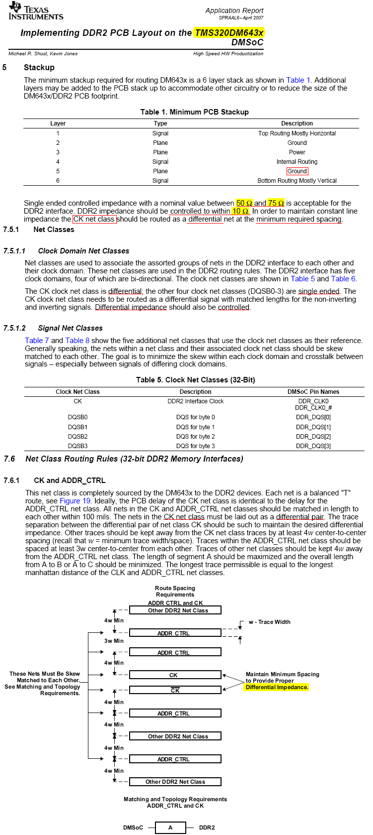
(1) Implementing DDR2 PCB Layout on the TMS320DM643x

DMSoC,

SPRAAL6


(2) Understanding TI's PCB Routing Rule-Based DDR Timing

Specification,

SPRAAV0A


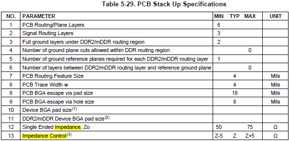
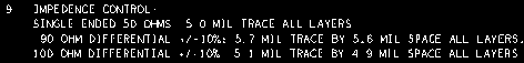
(1) contains lots of exact specifications such as wire impedance, net class, differential class, differential impedance and so on, many down to prescribed values; In contrast, (2) reads like a gentle introduction to novice users.

However, without figures as in (1), there is no way to determine whether the routed board matches basic DDR2 timing and routing constraints. So does a counterpart of (1) for OMAP L138 exist?


Zheng

  • It's in the OMAP-L138 data sheet, starting at page 126.

    -Mike

  • Anonymous
    0 Anonymous in reply to Michael Shust

    Michael,

    I got it, thanks.


    Zheng

  • Anonymous
    0 Anonymous in reply to Michael Shust

    Michael,

    I have some following-up questions:

    L138 datasheet page [127-139] contains specifications on many aspects of DDR2/mDDR memory. However, on the important specification of trace impedance, only on page 131, Table 5-29 did I find numeric information, yet it is only for single-ended traces:

    For (DDR_CLKP, DDR_CLKN) pair which from EVMAM1808 layout and Gerber file we could see having differential impedance of 100Ω, there is no information in L138 datasheet specifying the required differential impedance. What I only found was Table 5-33, which defined (DDR_CLKP, DDR_CLKN) as belong to clock net class CK, but this is not an electrical specification.

    Although it is almost guaranteed that EVMAM1808's 100Ω value is correct, I would still like to find this specification from TI documents for added assurance. Where can I get it?


    Zheng

  • Impedance of the DDR differential signals is specified by the single ended impedance and the requirement to route the differential pair at 2x center to center spacing.  The absolute impedance value is not as important as routing the signals close together to maximize noise rejection.

    -Mike

  • Anonymous
    0 Anonymous in reply to Michael Shust

    Michael,

    Michael Shust said:

    route the differential pair at 2x center to center spacing.

    I don't really understand this. Could you explain what is "2x center to center spacing"?


    Zheng

  • I should have written it as 2w center to center, that is how it is written in the data sheet.  w is the trace width.  Traces routed at 2w center to center will have a gap of width w between them.  Another way of specifying this would be to specify an edge to edge gap of 1w.

    -Mike

  • Anonymous
    0 Anonymous in reply to Michael Shust

    Michael,

    I got it, thanks very much for explanation.

    Zheng

  • Anonymous
    0 Anonymous in reply to Michael Shust

    Michael,

    In EVMAM1808 board layout file I found the following requirements:


    Width

    Space

    Required ZO

    Single-ended

    5.0


    50 Ω

    Differential

    5.1

    4.9

    100 Ω

    I noted two points:

    Z0:

    By the above standard formula for single-ended and differential impedance which can be found at Impedance Calculators - Mantaro Product Development Services, Zdiff would never be exactly 2Z0 unless d/h=∞, which requires h→0. The ratio of 2:1 = 100:50 in EVMAM1808 is by using width different than single-ended traces (5.1diff  vs 5.0single-ended). This however violated the rule you gave in two aspects:

    Rule

    Violation

    Impedance of the DDR differential signals is specified by the single ended impedance

    5.1≠5.0

    an edge to edge gap of 1w.

    5.1≠4.9

    Does it matter or not?


    Minimum impedance

    In L138 datasheet table 5-29, the minimum of Z0 would be 50Ω. However, EVMAM1808 specified nominal 50Ω impedance for Z0. Some PCB manufacturers told me that they could only guarantee the impedance fall within ±10% of the nominal range. So if -10% happens the actual Z0 would be 45Ω, below the minimum requirement.

    1. Would an actual 45Ω cause problem for DDR?
    2. Do I have to consider this tolerance in board fabrication to specify Z0-nominal × (1-10%) ≥ 50Ω ⟹ Z0-nominal ≥ 55.6Ω?


    Shape


    Equality

    Your rule above

    d = w

    EVMAM1808

    d(4.9) ≠ w(5.1)

    Possible alternatives

    d(4.8) ≠ w(5.2)

    d(4.3) ≠ w(5.7)

    ...

    d(5.2) ≠ w(4.8)

    d(5.3) ≠ w(4.7)

    ,etc.

    As already mentioned above, EVMAM1808 uses unequal w and d which is different from your rule. Manufacturers also suggested adjusting w and d with like (d=4.8, w=5.2) and other values with even larger difference between w and d values. I don’t know the physics here, but is there any rigid rule requiring w = d here, or unequal values can be used to obtain required Zdiff as defined in formula [1] above?


    Trapezoidal trace

    Manufacturers told me that due to the etching process, all traces would eventually have trapezoidal shape. The following illustration is from Polar instruments:

    With this real-world trapezoidal shape, do you define w = (w1 + w2) / 2 ? Do you measure d in Zdiff from bottom or middle of the traces? Is there still any requirement for w = d?


    Zheng

  • The controlling spec is the OMAP-L138 data sheet.

    The PCB fab shop will handle getting the correct PCB dimensions to hit the impedance spec from the data sheet.  That is one of the things you are paying them for.

    I think you are overcomplicating this.

    -Mike 

  • Anonymous
    0 Anonymous in reply to Michael Shust

    Michael,

    I will discuss with PCB fab houses on this.

    Zheng