This thread has been locked.

If you have a related question, please click the "Ask a related question" button in the top right corner. The newly created question will be automatically linked to this question.

AM335x unable to read LCD registers while debugging

Other Parts Discussed in Thread: SYSCONFIG

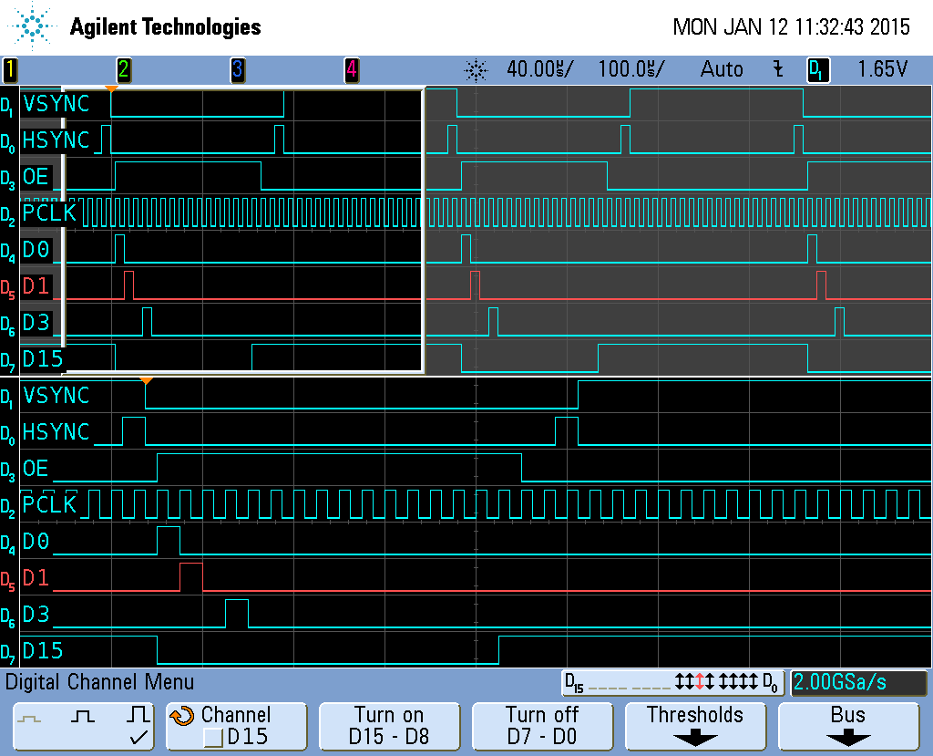
As part of a project, I am trying to write bare metal code to drive a BeagleBone and DVI cape to emit a video signal. As part of this process I am trying to figure out how to configure the AM335x's LCD module.

I set bits 1:0 of CM_PER_LCDC_CLKCTRL to 0x2 to enable the LCD module. (The power mode SFRs are already properly configured, it seems). When I do this it seems that STBYST and IDLEST both immediate go to 0x0 (module is functional). I then try setting the LCD module's registers.

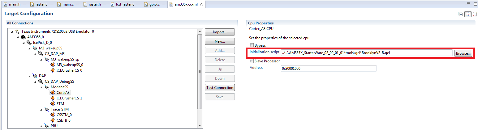
Unfortunately, this is very unreliable. I am working with CCS v5.3, which has a 'Registers' window allowing one to view the values of SFRs when the program execution is halted. However, the debugger is usually unable to read the LCD controller SFR registers (value is marked as "Error: unable to read"). Sometimes proceeding through the code will trip the error interrupt (UndefInstHandler), sometimes it will not. Sometimes upon enabling the module a few of the SFRs resolve to readable values in the 'Registers' window, but trying to set bits causes the processor to crash.

Is this a limitation of the CCS debugger? Am I initializing the LCD module correctly, or is there more to enabling it? Any help or insight would be greatly appreciated.

  • Hi Austin,
     
    About programming sequence of the LCD controller, please read section 13.4 of the AM335X Technical Reference Manual.
  • Hi Austin,

    Were you ever able to get the BeagleBone DVI-D to work?  I am trying to set a video mode in SYS/BIOS, and I am not sure what driver to use as a base for my work.


    Thanks!

    Noel

  • Hi All,

    I am also working on drive a  BeageBone DVI cape using starterware "AM335X_StarterWare_02_00_00_07",  am trying display image.h on the LCD screen which is connected to BeageBone DVI-D cape with HDMI cable. But this starterware don't have ratster application for BeagleBone board .

    Can I use evmAM335x raster application for BeagleBone DVI-D cape?????

    Thanks

    Ram

  • Hello,

    I am having exactly the same issue as Austin has experience, though I am using CCSv6 and AM335x StarterKit.

    Any insight or suggestion?


    Thanks,

    Dawei

  • The module definition file (ccs_base/common/targetdb/Modules/am335x/LCD.xml) includes registers which are hazardous to read, especially the LIDD ADDR and DATA registers. Since they are simply marked as read/write registers, merely opening the register view in CCS will trigger reads to them, which no doubt creates a big mess.

  • I'm deeply sorry for leaving this question hanging (c.f. this XKCD comic). I never did figure this out and I eventually shelved the side project it was part of. One of my goals this year is to revisit this project and try to get bare metal code writing to the LCD via DVI; if I'm successful I'll post how I did it here.

    In the meantime, it does seem that the registers in question are privileged, and so they can't be properly examined using the development tools.

  • Austin Zheng said:
    I'm deeply sorry for leaving this question hanging (c.f. this XKCD comic).

    Hah, nice reference. Unfortunately I think there are many such threads on e2e. I have witnessed cases where someone posted the solution they eventually found to their problem, months after starting the thread, but this is very rare. Typically threads just die, and annoyingly the next person with the same problem often makes a new thread rather than bumping an existing one (thus ensuring that even if a solution is found this time, people who previously had the problem probably won't learn about it any time soon).

    Austin Zheng said:
    In the meantime, it does seem that the registers in question are privileged, and so they can't be properly examined using the development tools.

    Yes, I think commenting out the offending registers in the xml file would be a good start... read-unsafe registers simply don't belong in a debug view. Based on a quick look it seems the four LIDD_CS{0,1}_{ADDR,DATA} registers may actually be the only problematic ones, but I haven't tried anything (or ever used the LCD controller myself).

  • Thanks Anstin and Matthijs.This kind of things does happen from time to time in e2e forum. I wish TI could put more staffs/resources to help out their customers.

    I'll give it a try and let you know if there is any update. Meanwhile I will seek help and confirm it from our local TI support.

  • BTW, it's worth mentioning that the Freon/Primus dies (OMAP-L1xx / TMS320C674x / AM1xxx) have an older version of the same LCD controller peripheral (except parts whose last digit is 2 or 5), and its TRM chapter explains some settings in more detail than the AM335x TRM does.

    Overall it doesn't look like a very hard peripheral to set up, although the effect of some of the data layout config bits isn't really clear to me, especially the big-endian setting of the DMA controller.  It doesn't help that the peripheral is native to DSP-like chips which tend to have configurable endianness and I think their (CBA / VBUS / TeraNet) interconnect technology is endianness-aware, while neither is the case on the AM335x, so I don't know if DMA controller performs a byte-swap, halfword-swap, or just passes the bit as metadata to be subsequently discarded by the interconnect.

    I don't have a display to connect to it, but you get points with me for referencing xkcd ;-) so I'll see if I can at least get it running without errors.

  • Matthijs van Duin said:
    Overall it doesn't look like a very hard peripheral to set up

    And in fact it wasn't:

    Of course this is a slightly silly configuration: display PLL still in bypass (24 MHz clock) and divided down to a 100 kHz pixel clock.  All other timing parameters are left at zero, so that yields a magnificent 16×1 pixel display ;-)   My steps were:

    • PRCM: enable lcdc clock domain (0x148) and module (0x18), wait until module ready
    • I've noticed LCDC fully supports byte- and halfword-writes (except to write-1-to-clear regs as usual) so I've split CTRL into: u8 global_mode; u8 clock_div;
      • set global_mode to 1 to select raster mode
      • configure clock_div to some value in range 2 .. 255 (I used 240 for this test)
    • enable clocks to DMA and raster controller (CLKC_ENABLE = 5)
    • configure raster controller.  I just set RASTER_CTRL to (1 << 7 | 1 << 23) to select 16-bit active-matrix, but you'll want to set the remaining RASTER_* registers to sensible values too obviously.
    • configure pinmux.  A reason not to do this earlier is because the settings done above will affect the idle-level driven onto the pins.
    • select 16-bit color (no palette mapping) by loading the trivial "palette": u16 palette[16] alignas(4) = { 0x4000 };
      • make sure it's at least word-aligned (I used the C++ alignas-directive there)
      • make sure it's in some place the lcdc can access such as OCMC ram or external ram (not mpuss-local ram)
      • make sure it has actually arrived there. assuming the memory region is non-cacheable a data sync barrier (gcc: asm( "dsb" ::: "memory" ); ) followed by reading back any part of it will guarantee this (use a volatile read to ensure it's not optimized away)
      • configure the palette buffer into FB0_BASE and _CEILING (note: ceiling = base + size)
      • configure raster controller for "palette loading only".  I also set reqdly to its max value to ensure there's no chance of underrun (not that that's a risk with the silly slow clock I used anyway).  Since this is done only once during setup it's not performance-critical anyhow.
      • enable raster controller.
      • wait for palette-loaded event (you can use an irq or just poll)
      • disable raster controller and clear irqs.
    • program actual frame buffer (same considerations as above), select "data loading only", enable raster controller.

    That's it, controller operational!  Since I had only 16 pixels and 16-bit color I reused the palette buffer as frame buffer, but filled with test data: buf[i] = 1 << i;

    Some observations:

    • There is no way whatsoever to reset the lcdc registers.  Its sysconfig lacks a reset-bit, the CLKC_RESET bits apparently only affect functional logic, not even an OCP reset via the LCDC's target agent had any effect on the config registers.  This means that if some earlier code meddled with the LCDC (e.g. a bootloader felt the need to display a splash screen) you need to carefully disable it and ensure the correct values of all registers.  Disabling it requires care according to the docs: if it's doing a palette-only load you should wait for completion before disabling, otherwise you should disable and wait for the completion event (bit 0 of irq_rawstatus).  Only then can you reset the functional logic if you feel a need to.  ... fussy thing.
    • There are many mentions in the subarctic TRM of passive-matrix mode having 15 grayscale levels or 153 = 3375 colors even though table 13-10 shows 16 distinct levels.  Comparison with the freon/primus TRM solved this mystery: its ditherer indeed only supported 15 levels. It was apparently upgraded to support 16 levels in subarctic but they neglected to fix all occurrences of 15 → 16 and 3375 → 4096.
    • section 13.4.4 clarified the various endian-bits:  the DMA controller can swap halfwords of each word (cfg_bigendian) and/or bytes of each halfword (cfg_byte_swap). Moreover, for palette-mapped modes, the raster controller can reverse the order of the pixels (cfg_rdorder=1) of each halfword (cfg_nibmode=0) or of each byte (cfg_nibmode=1).

    Hope this helps!

  • Thanks for the suggestions. I found out AM18x LCD user guide has a much more detailed explanation for configuration of each register. The difference of LCD controller between AM18x and AM335x are very little: 1) AM335x supports 24 bit frame buffer, 2) AM335x supports LCD interrupts. But the latter is not necessary if you simply want to bring up the LCD display function.

    You are right about those LCD SFRs - They cannot be monitored from register view in CCS while being read/written. Once I removed those LCD registers from the watchlist, I was able to proceed. Speaking of setting DMA controller, however, I don't think that is necessary either, at least I was able to make it work without the DMA controller.
  • I would also like to share my codes to make the LCD running. It is not perfect yet, but at least my bare metal codes were basically working. I found a lot of helpful info from AM335x StarterWare and TI WiKi, i.e. GEL scripts and doc about programming LCD registers, as well as setting up DDR2 memory properly.


    Environment: one custom PCB with AM335x and DDR2 SDRAM,  one 3.5" LCD with 320x240 and 16BPP mode, and Code Composer Studio v6. In my case, AM335x MPU is running at 300MHz, DDR2 clock running at 150MHz, and LCD pixel at 5MHz.. They can be set to any frequency to tailor your application though. Right now I was able to display a test pattern with color strips on the screen.


    1. I modified AM335x_EVM.gel a little bit so as to initialize the processor in CCS.  This includes setting up OPP100 mode by configuring 5 PLLs including display PLL, and also set up EMIF for DDR2 SDRAM. Not sure if each of PLLs has to be configured, but I did all since they will be useful for  future development  anyway.


    I set up Display PLL with 50MHz output as LCD_CLK. It serves as input clock to LCD peripherals, which I further divided down to 5MHz as pixel clock. Note on AM335x StarterKit it was using output of Perihperal PLL at 192MHz as LCD clock input, but this should work the same way.


    Configuring EMIF is necessary as it's the storage address for LCD frame butter (usually starting at 0x80000000). I believe following the steps in the TI Wiki page below will make your DDR2 up running. Eventually in Memory Browser of CCS, you should be able to navigate to address at 0x80000000 and write to any address after it.

    http://processors.wiki.ti.com/index.php/AM335x_EMIF_Configuration_tips

    Note: ARM mode in CPSR register should be set to "privilege (0b10111)" instead of "user (0b10000)", or else writing to EMIF registers won't work. I haven't figure out an easier way to do it. Thus each time I launched the debug mode, I had to set it manually in Register View window.

    2. Create CCS Project with AM335x. Then I attached the GEL as init script of AM335x.ccxml so that both the processor and DDR2 interface could be automatically initialized each time CCS is connecting to a target board in debug mode. It is in AM335x.ccxml->"Target Configuration" and looks like this:

    3. Run codes to init the LCD peripheral. Page#112 of AM335x StarterKit User Guide explains details of  programming sequence for raster LCD. More codes could be found from AM335x StarterWare. I put my codes below for whoever might need it, but please bear with my non-standard coding style as being mostly a hardware engineer.

    Note: the codes I used won't make the LCD display perfectly, as I have seen some horizontal offset on the screen, but at least I was able to see something. I will update separately if I figured it out the root cause.

    ###################################################

    uint32_t Raster_Config_AM335x(void)
    {
    	uint32_t x;
    	uint16_t *pdata;
    
    	/* refer to AM335x StartWare UserGuide_02_00_00_07.pdf for programming sequence of raster controller. */
    
    	// Configure required clock for LCDC instance
    	LCDModuleClkConfig();
    
    	// Pinmux setting, not necessary if you have done it earlier
    //	LCD_PinMux_Setup();
    
    	// Enable Software Clock for DMA,LIDD submodule and for Core(which encompasses raster active and passive matrix logic) by invoking RasterClocksEnable() API
    	WR_MEM_32(LCD_CLKC_ENABLE, 0x7);			// enable DMA, LIDD, CORE clock
    
    	// Disable Raster mode
    	WR_MEM_32(LCD_RASTER_CTRL, RD_MEM_32(LCD_RASTER_CTRL) & 0xFFFFFFFE);
    
    	// clear IRQ status
    //	WR_MEM_32(LCD_IRQENABLE_CLEAR, 0x3FF);
    
    	// Configure the rate at which pixel data should be output by configuring pixel clock frequency
    	WR_MEM_32(LCD_LCD_CTRL, 0x00000A01);		// clkdiv = 10 > PCLK = 5MHz given LCD_CLK = 50MHz; Raster mode;  restart module on a underflow
    
    	// Configuring the DMA for single or double frame buffer ,busrst size for DMA data transfer etc
    	WR_MEM_32(LCD_LCDDMA_CTRL, 0x00000000);		//  frame buffer 0 is used; burst size of 1 word; 8 dword FIFO buff
    
    	// Configuring Panel type(TFT or STN) ,color display or monochrome, 1/2/4/8/16/24 bit per pixel mode
    	WR_MEM_32(LCD_RASTER_CTRL, 0x00200080);		// disable raster, TFT 16 bit frame butter
    
    	// Configure the polarity of various timing parameters (for example frame clock , pixel clock, line clock etc.)
    	WR_MEM_32(LCD_RASTER_TIMING_2, 0x03000000);	// Hsync/Vsync falling edge synced by PCLK at its rising edge
    
    	// Configure the Horizontal timing parameters and pixel per line of the raster
    	WR_MEM_32(LCD_RASTER_TIMING_0, (0x1D << 24) | (0x1D << 16) | (0x1D << 10) | (0x13 << 4) ); 	// HBP = 0x1D (30-1); HFP = 0x1D (30-1); HSW = 0x0; PPL = 0x13
    
    	// Configure the vertical timing parameters and Pixel per panel of the raster
    	WR_MEM_32(LCD_RASTER_TIMING_1, (0x03 << 24) | (0x03 << 16) | (0x03 << 10) | (0xEF) ); 		// VBP = 0x3 (4-1); VFP = 0x3 (4-1); VSW = 0x0: LPP = 0xEF;
    
    	// Configure the required amount of FIFO delay (e.g. 128)
    //	WR_MEM_32(LCD_RASTER_CTRL, RD_MEM_32(LCD_RASTER_CTRL) | 0x80 << 0xC);
    
    	// Configure the base/ceiling address register with base address of the array
    	WR_MEM_32(LCD_LCDDMA_FB0_BASE, FRAMEBUF_BASE);	// Starting address for DDR2 SDRAM
    	WR_MEM_32(LCD_LCDDMA_FB0_CEILING, FRAMEBUF_BASE + (32 + (LCD_WIDTH * LCD_HEIGHT -1 )* 2 )); // Frame buffer end)
    
    	// Enable End of frame 0 interrupts
    //	WR_MEM_32(LCD_IRQENABLE_SET, 0x100);
    
    	/* Palette */
    	pdata = (uint16_t *)FRAMEBUF_BASE;
    	*pdata++ = 0x4000;
    	for (x = 0; x < 320*240; x++)
    	      *pdata++ = 0x0000;
    
    	WR_MEM_32(LCD_RASTER_CTRL, RD_MEM_32(LCD_RASTER_CTRL) | 0x1);		// enable raster controller
    
    	   return (ERR_NO_ERROR);
    }

    void LCDModuleClkConfig(void)
    {
    	WR_MEM_32(CM_PER_L3S_CLKSTCTRL, 0x2);		// SW_WKUP for CLKTRCTRL. Start a software forced wake-up transition on the CM_PER domain.
    	while(0x2 != ( RD_MEM_32(CM_PER_L3S_CLKSTCTRL) &  0x3));
    
    	WR_MEM_32(CM_PER_L3_CLKSTCTRL, 0x2);
    	while(0x2 != ( RD_MEM_32(CM_PER_L3_CLKSTCTRL) &  0x3));
    
    	WR_MEM_32(CM_PER_L3_INSTR_CLKCTRL, 0X02);
    	while(0x2 != ( RD_MEM_32(CM_PER_L3_INSTR_CLKCTRL) &  0x3));
    
    	WR_MEM_32(CM_PER_L3_CLKCTRL, 0X02);
    	while(0x2 != ( RD_MEM_32(CM_PER_L3_CLKCTRL) &  0x3));
    
    	WR_MEM_32(CM_PER_OCPWP_L3_CLKSTCTRL, 0x2);
    	while(0x2 != ( RD_MEM_32(CM_PER_OCPWP_L3_CLKSTCTRL) &  0x3));
    
    	WR_MEM_32(CM_PER_L4LS_CLKSTCTRL, 0x2);
    	while(0x2 != ( RD_MEM_32(CM_PER_L4LS_CLKSTCTRL) &  0x3));
    
    	WR_MEM_32(CM_PER_L4LS_CLKCTRL, 0x2);
    	while(0x2 != ( RD_MEM_32(CM_PER_L4LS_CLKCTRL) &  0x3));
    
    	/* lcd pixel clock is derived from Display PLL */
    	WR_MEM_32(CM_DPLL_CLKSEL_LCDC_PIXEL_CLK, 0x0);		// 0x0 for DISP PLL; 0x1 for CORE PLL; 0x2 for PER PLL
    
    	WR_MEM_32(CM_PER_LCDC_CLKCTRL, 0x2);
    	while(0x2 != ( RD_MEM_32(CM_PER_LCDC_CLKCTRL) &  0x3));
    
    	while(!( RD_MEM_32(CM_PER_L3S_CLKSTCTRL) &  0x8));	// check clock status in CM_PER_L3S
    
    	while(!( RD_MEM_32(CM_PER_L3_CLKSTCTRL) &  0x10));	// check clock status in CM_PER_L3
    
    	while(!( RD_MEM_32(CM_PER_OCPWP_L3_CLKSTCTRL) &  0x30));	// check clock status in OCPWP L3 and OCPWP L4
    
    	while(0x20100 !=( RD_MEM_32(CM_PER_L4LS_CLKSTCTRL) &  0x00020100)); 		// check clock status in CM_per_L4LS_CLKSTCTRL for LCDC_GLCK, and L4LS_GCLK
    }

    #####################################################

    Once raster controller is enabled, you should be able to see all 3 clocks (Pixel, HSYNC, VSYNC) from the scope.

  • Dawei Liu said:
    The difference of LCD controller between AM18x and AM335x are very little: 1) AM335x supports 24 bit frame buffer, 2) AM335x supports LCD interrupts.

    Freon's LCDC supports interrupts too, but its irq status register is at offset 0x8 while irq-enable bits are scattered across the module, Subarctic gathered these into a standard irq block apended at the end, along with local clock/reset controls. There are other differences: Subarctic was upgraded to support 2048×2048 displays (from 1024×x1024), some wider range of other timing settings, support for auto-restarting the next frame after a fifo overrun, 16-level rather than 15-level passive matrix ditherer, and there may be other differences I haven't noticed.  Still, the basics are still the same and compatible, apart from how to enable/test/clear irqs (you still need to account for the status register having moved even if not using irqs).

    Dawei Liu said:
    Once I removed those LCD registers from the watchlist, I was able to proceed. Speaking of setting DMA controller, however, I don't think that is necessary either, at least I was able to make it work without the DMA controller.

    Well my impression was that people were trying to get raster mode operational (at least one poster mentioned this explicitly and nobody mentioned lidd mode), which is also what I did, and raster mode only works with the LCDC's integrated DMA controller.

  • Dawei Liu said:
    I would also like to share my codes to make the LCD running. It is not perfect yet, but at least my bare metal codes were basically working. I found a lot of helpful info from AM335x StarterWare and TI WiKi, i.e. GEL scripts and doc about programming LCD registers, as well as setting up DDR2 memory properly.

    I'll see if I can clean up my code a bit and post it too, it's very different in style though which may either appeal or appall people ;-)  I avoid relying on GEL scripts since a finished application can't make use of them either.  My Makefile generates an MLO which can be directly loaded by boot ROM (in addition to the ELF executable which you can still upload via JTAG during development/debugging of course).  I don't use any code from StarterWare, the few experiences I have with it are not very positive (at best the code is often very inefficient, some other code I've seen is horribly broken such as the UART driver and example).

    My code doesn't include EMIF initialization yet though, so that imposes a rather severe limit on the size of the frame buffer (it needs to fit in internal SRAM alongside the code).  It does include full initialization of the cortex-A8 cpu (including MMU and caches) and a simple IRQ-driven GPIO example. [Edit: I just noticed I disabled that, so it's not included in the sizes mentioned. The IRQ controller still initialized though.]  Total size of the produced MLO is 1 KB exactly (972 bytes when LTO is enabled, 896 bytes when optimizing for size), so in principe all 64 KB of the OCMC could be available as frame buffer without initializing EMIF (though this would require some changes to the linker file since currently I'm putting the code in OCMC rather than MPUSS ram).

    Dawei Liu said:
    I set up Display PLL with 50MHz output as LCD_CLK. It serves as input clock to LCD peripherals, which I further divided down to 5MHz as pixel clock. Note on AM335x StarterKit it was using output of Perihperal PLL at 192MHz as LCD clock input, but this should work the same way.

    It's worth mentioning the Peripheral PLL is a low-jitter PLL (ADPLL-LJ) while the display PLL is not (ADPLLS).  If you can make your pixel clock from the 192 MHz (or 96 MHz at OPP50) peripheral clock then I think that option would be preferred.  This frees up the display PLL to be either unused (lower power consumption) or used as alternative clock source for PRU-ICSS, which probably needs unusual clock rates in various use cases (when it's being used to emulate a controller for some bus with specific timings).

    Dawei Liu said:
    Note: ARM mode in CPSR register should be set to "privilege (0b10111)" instead of "user (0b10000)", or else writing to EMIF registers won't work. I haven't figure out an easier way to do it. Thus each time I launched the debug mode, I had to set it manually in Register View window.

    The best solution is finding whatever piece of StarterKit is responsible and don't call it. If I remember correctly, starterkit also includes a function to request re-elevation to privileged state. I don't know how to do it from GEL but I do know how to do it from the newer debug server scripting:  session.memory.writeRegister( "CPSR", 0x40000193 );

    A better solution however is to always reset the target before reuploading, since this ensures both CPU and all peripherals are in a known state.  Othewise your code will also have to deal with fixing any settings which may have been done by a previous iteration of your code, including carefully disabling and reinitializing the LCDC, since it would still be running, and my impression from docs is that this needs to be done carefully to avoid confusing the controller (which, as I noticed, lacks any genuine local reset).

  • Thanks for continuing share your insights. But first off, I have to say it is not me but Austin Zheng, who posted the xkcd cosmetic, that deserves your points :-).

    My impression about the difference of LCDC, which I now know is incomplete, actually came from scattered codes in StarterWare. I actually had a lot of trouble understanding the GELs and "free" codes coming with it. Some of the register values are still not correct and TI had very little document/support for it. Eventually I sat down with both TRM and StarterWare codes open, going through the codes line by line in an attempt to understand configuration for each register.  That's typically how I made it work.

    Could you tell me what SDE you were using for this experiment? You seems to know the processors very well. Honestly I don't understand some of your words, especially how you set up the experiment earlier without using external RAM. So far my understanding of AM335x stays at very superficial level, i.e. read/write to registers in CCS through C language, without deep understanding of the processor architecture or how a compiler works at lower layer, let alone make it more efficient or flexible from a system perspective. I tried to search for documentation to learn, but in general they are very limited. For example, TI has intended to hide the docs for L3/L4 and OCP, thus I was not able to understand what clock LCDC requires, and how to configure among many scattered registers.

    Matthijs van Duin said:
    Well my impression was that people were trying to get raster mode operational (at least one poster mentioned this explicitly and nobody mentioned lidd mode), which is also what I did, and raster mode only works with the LCDC's integrated DMA controller.

    I thought you were talking about enhanced DMA. You are right. I was using the integrated DMA with the raster controller, or else the frame butter shouldn't function.

  • Dawei Liu said:
    I have to say it is not me but Austin Zheng, who posted the xkcd comic, that deserves your points :-).

    I know, and he provided the motivation -- if you others like you benefit from it as well, that makes it even more worthwhile :-)


    Dawei Liu said:
    My impression about the difference of LCDC, which I now know is incomplete, actually came from scattered codes in StarterWare. I actually had a lot of trouble understanding the GELs and "free" codes coming with it. Some of the register values are still not correct and TI had very little document/support for it. Eventually I sat down with both TRM and StarterWare codes open, going through the codes line by line in an attempt to understand configuration for each register.

    The messy situation has been motivating me to work on some baremetal examples, but I have limited time available for them. I hope to eventually set up a git repository with them.

    Most of my baremetal experience actually comes from its architectual ancestor, Centaurus (DM814x / AM387x), which has no StarterWare at all. I've looked at AM335x StarterWare a few times now, usually because people were having trouble with it, and so far it usually made me facepalm. Some of that stuff looks like whoever wrote it was pretty confused too, which doesn't make it the best source for achieving enlightment yourself obviously.

    My main source is info is still the TRM. I also tend to browse TRMs of related processors since the amount of attention a particular aspect of the TRM gets seems to vary a lot. The "flagship" products often have detailed documentation, such as the OMAPs before that division was killed off, with the OMAP 4 being most closely related.  Sometimes strange aspects of a peripheral can become a lot clearer when you know its history (such as the "3375 colors" claim of passive-matrix mode in the subarctic LCDC being inexplicable to me until I learned that its predecessor's ditherer only supported 15 levels). Being at least superficially familiar with the other docs also makes it easier to spot when a section of documentation has been inappropriately copy-pasted from another processor without account for the relevant differences.

    I also keep every version of documentation I download, since they are not merely enhanced but stuff can also disappear if TI feels it is not relevant/appropriate for their audience to which they are marketing the processor, or they do not wish to publicly support it.  The chapter about PRUSS for example disappeared after revision C (2011-12) before reappearing in revision K in 2014-06 (although in the meantime a limited subset was released separately as "unsupported documentation").  The already very inadequate chapter about the L3 and L4 interconnects also got even less informative over time.

    BTW, you may have noticed by now I prefer the die names over their part codes. This is because I think they are much more memorable and easier to distinguish than part codes, especially since completely different dies can have very similar looking part codes (think am335x vs am35xx) while the same die can have very different part codes if some part of is disabled (didn't pass test) and it lands in a different marketing segment. A quick reference table of a few dies which have a Sitara incarnation (sorted roughly in chronological order):

    Freon OMAP-L13x, C674x, AM1xxx (when last digit is even)
    Primus OMAP-L13x, C674x, AM1xxx (when last digit is odd)
    Netra DM816x, AM389x, C6A816x
    Centaurus DM814x, DM812x, AM387x, DRA65x, DRA64x, TDA1Mxx
    Subarctic AM335x, DRA60x, DRA61x
    Aegis AM437x
    Vayu AM57xx, DRA7xx, TDA2xx

    The AM-versions of Freon/Primus can also be distinguished by the second digit: AM18xx vs AM17xx. The Vayu part code ranges may be too broadly masked, it's always possible other dies are later inserted into those ranges (e.g. discovering subarctic in the DRA6xx series came as a surprise to me). Automotive parts (DRA / TDA) have very limited public info, so mistakes there are quite possible.

    AM35xx and AM37xx are not in the list since I don't know their names (assuming they have one). AM37xx is just a feature-reduced OMAP36xx (and the only OMAP I know by name is the OMAP 4 "Phoenix"), while AM35xx is slightly unusual in being clearly OMAP3-derivative yet also significantly modified to suit broadmarket applications.

    Vayu is OMAP5-derivative and was apparently also an OMAP-to-be (OMAP5777) but will presumably never get released as such.  The range from Netra to Aegis are all architectural siblings, and to a lesser degree related to the OMAP 4.  Freon/Primus are very similar to each other but very unlike the rest of the list, they are I guess more related to the older DaVinci members or maybe even the Keystone series.

    Dawei Liu said:
    Could you tell me what SDE you were using for this experiment?

    SDE? Software development environment?  Just a decent text editor (vim) and a handwritten Makefile.  Since there've been a lot of useful additions in recent C++ versions (especially some type inference and better metaprogramming support) I use the latest GCC release (4.9.2), originally the one from linaro although I later compiled my own toolchain using Crossbuild: LTO (link-time optimization) was broken in the linaro build, and building my own toolchain allowed me to make sure everything was optimized for the cortex-a8 (which is the oldest of the cortex series) while linaro seemed to focus more on the latest processors.

    Since CCS is very slow on my computer and a memory hog I usually don't start it unless absolutely necessary.  I also dislike it (and other IDEs I've encountered) since it makes everything very untransparent to me.  Often I have no idea where to look in its zoo of settings to fix something that isn't doing what I want it to do.  I upload code using debug server scripting.  I still have on my to-do list to give OpenOCD another chance so I can avoid having to use CCS when I need to step through my code (although OpenOCD has plenty of issues too).

    You can find a small demo project I wrote (from which my LCDC test also indirectly derives) linked to in this thread.

    Dawei Liu said:
    You seems to know the processors very well. Honestly I don't understand some of your words, especially how you set up the experiment earlier without using external RAM.

    There are various internal RAMs, the most important ones here being the 64 KB RAM embedded in MPUSS (where the Cortex-A8 resides) which is at 0x402f0000 - 0x402fffff although the first 1 KB is accessible due to being reserved for secure-world (which doesn't use it, but reserves it anyway), and the 64 KB OCMC (On-Chip Memory Controller) RAM which is at 0x40300000 - 0x4030ffff.  Since these memory regions are directly adjacent they can be treated as a single 128 KB region, which is what the ROM bootloader does.  Code loaded by the ROM bootloader is loaded into this region (a header before the the code specifies where exactly) and then executed.  Such code is known as the MLO (since when booting from MMC it looks for a file named "MLO") or SPL ("secondary program loader"), which refers to the typical case where this code only has the task of initializing external RAM and then loading the application or yet another intermediate bootloader.  If the application is sufficiently small (as it is here) it can of course also be directly loaded as "MLO" by the ROM bootloader.  More details on this process can be found in the Initialization chapter of the TRM.

    Even though ROM may treat the two memories are a single region, the are actually some big differences between them: the cortex-a8 obviously has very low-latency access to its local RAM, but only the cortex-a8 can access it, while the OCMC RAM is hooked up to the L3 interconnect and is accessible to all initiators. This means that for example the frame buffer for LCD can be placed in OCMC ram but not in MPU ram.  Also, when jtag-debugging, you can inspect OCMC ram via DAP while the cpu is running, while inspecting the MPU RAM requires halting the cpu (and is much slower).

    So far my understanding of AM335x stays at very superficial level, i.e. read/write to registers in CCS through C language, without deep understanding of the processor architecture or how a compiler works at lower layer, let alone make it more efficient or flexible from a system perspective. I tried to search for documentation to learn, but in general they are very limited. For example, TI has intended to hide the docs for L3/L4 and OCP, thus I was not able to understand what clock LCDC requires, and how to configure among many scattered registers.

    I'll try to finish up my LCD example: since it's very minimalistic it may help making the process clearer (despite my eccentric dialect of C++).  You can also look at the irq-driven GPIO example I gave in the thread I mentioned earlier, it has the same style (and same compiler requirements).

    The interconnect is actually not responsible for clock distribution, that's covered by PRCM.  Subarctic's PRCM register map is however an unbelievable mess.  It looks like it was organized by someone who was drunk, but more likely it wasn't organized by a human being at all but stuff was just automatically allocated during the design process.  The longer you look at it, the more ways you discover in which it manages to be inconsistent.  *deep sigh*

    If you do want to know more about the interconnect (but you don't strictly need it here), I suggest centaurus' TRM, chapter 1.12, since it's very similar (except subarctic removed L3M, which had already kind of fused with L3F in centaurus, and added L4WK).  You can also find target IDs, locations of interconnect registers and firewalls, etc in my combined centaurus/subarctic memory map spreadsheet.

  • Matthijs van Duin said:
    locations of interconnect registers and firewalls, etc in my combined centaurus/subarctic memory map spreadsheet.

    Ah actually I just realized I haven't integrated those yet, but they are in this post from me.

  • Thank you Matthijs for those comments, suggestions, and directions. That's a lot of things I would need to take time to learn and digest. It may be a little off the topic now, but I appreciate your time very much. I will keep you posted if I run into any question down the road. Thanks again!

    -Dawei