Hello Everyone,
We got our production board which is same as DM8148 reference board. On the new board, only change is memory configuration, we upgraded it to 4GB of DDR3 SDRAM with 16x8 memory banks instead of 8x8 banks as in Ref board. On the production board we are able to run the flash programmer or any program from the internal SRAM using CCS with XDS510 debugger. But we are not able to proceed with TI u-boot (Ver 04.04.00.02) code as the memory configuration is different on the production board.
When we browse through the TI forums, found a procedure to do a software levelling http://processors.wiki.ti.com/index.php/TI814x-DDR3-Init-U-Boot which is a necessary thing to configure the DDR3 memory. When I run the DDR3_SlaveRatio_ByteWiseSearch_TI814x.out from CCS, I am getting the ratio values as 0s. So I am not able to proceed further from this point. I have captured the log of Slave_Ratio tool. Please check it below.
Can you please through some light to resolve this issue? And we just wanted to know that, is this a correct way to do the memory configuration? Or is there any other way/ tools available to do SDRAM configuration?
Looking forward to hear from you.
Thanks & Regards
Vinod
#### Log #####
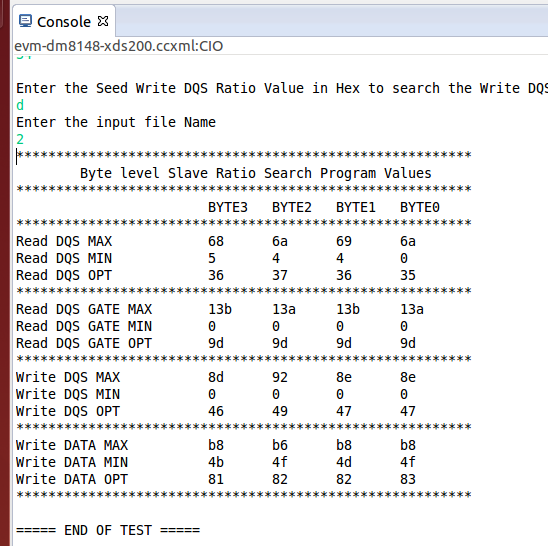
[CortexA8] Enter 0 for DDR Controller 0 & 1 for DDR Controller 1
0
[CortexA8] DDR START ADDR=0x80000000
[CortexA8]
[CortexA8] Enter the Seed Read DQS Gate Ratio Value in Hex to search the RD DQS Gate Window
0xb3
[CortexA8]
[CortexA8] Enter the Seed Read DQS Ratio Value in Hex to search the RD DQS Ratio Window
0x34
[CortexA8]
[CortexA8] Enter the Seed Write DQS Ratio Value in Hex to search the Write DQS Ratio Window
0x08
[CortexA8] Enter the input file Name
ti_ddr.txt
[CortexA8] RD DQS RATIO MINIMUM VALUE DIDN'T CONVERGE
[CortexA8] RD DQS RATIO MINIMUM VALUE DIDN'T CONVERGE
[CortexA8] RD DQS RATIO MINIMUM VALUE DIDN'T CONVERGE
[CortexA8] RD DQS RATIO MINIMUM VALUE DIDN'T CONVERGE
[CortexA8] RD DQS RATIO MINIMUM VALUE DIDN'T CONVERGE
[CortexA8] RD DQS RATIO MINIMUM VALUE DIDN'T CONVERGE
[CortexA8] RD DQS RATIO MINIMUM VALUE DIDN'T CONVERGE
[CortexA8] RD DQS RATIO MINIMUM VALUE DIDN'T CONVERGE
[CortexA8] RD DQS GATE RATIO MINIMUM VALUE DIDN'T CONVERGE
[CortexA8] RD DQS GATE RATIO MINIMUM VALUE DIDN'T CONVERGE
[CortexA8] RD DQS GATE RATIO MINIMUM VALUE DIDN'T CONVERGE
[CortexA8] RD DQS GATE RATIO MINIMUM VALUE DIDN'T CONVERGE
[CortexA8] RD DQS RATIO MINIMUM VALUE DIDN'T CONVERGE
[CortexA8] RD DQS RATIO MINIMUM VALUE DIDN'T CONVERGE
[CortexA8] RD DQS RATIO MINIMUM VALUE DIDN'T CONVERGE
[CortexA8] RD DQS RATIO MINIMUM VALUE DIDN'T CONVERGE
[CortexA8] RD DQS RATIO MINIMUM VALUE DIDN'T CONVERGE
[CortexA8] RD DQS RATIO MINIMUM VALUE DIDN'T CONVERGE
[CortexA8] RD DQS RATIO MINIMUM VALUE DIDN'T CONVERGE
[CortexA8] RD DQS RATIO MINIMUM VALUE DIDN'T CONVERGE
[CortexA8] RD DQS GATE RATIO MINIMUM VALUE DIDN'T CONVERGE
[CortexA8] RD DQS GATE RATIO MINIMUM VALUE DIDN'T CONVERGE
[CortexA8] RD DQS GATE RATIO MINIMUM VALUE DIDN'T CONVERGE
[CortexA8] RD DQS GATE RATIO MINIMUM VALUE DIDN'T CONVERGE
[CortexA8] WR DATA RATIO MAXIMUM VALUE DIDN'T CONVERGE
[CortexA8] WR DATA RATIO MINIMUM VALUE DIDN'T CONVERGE
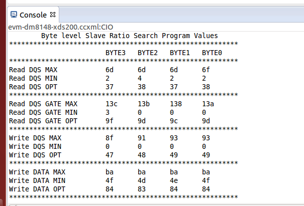
[CortexA8] *********************************************************
[CortexA8] Byte level Slave Ratio Search Program Values
[CortexA8] *********************************************************
[CortexA8] BYTE3 BYTE2 BYTE1 BYTE0
[CortexA8] *********************************************************
[CortexA8] Read DQS MAX 0 0 0 0
[CortexA8] Read DQS MIN 0 0 0 0
[CortexA8] Read DQS OPT 0 0 0 0
[CortexA8] *********************************************************
[CortexA8] Read DQS GATE MAX 0 0 0 0
[CortexA8] Read DQS GATE MIN 0 0 0 0
[CortexA8] Read DQS GATE OPT 0 0 0 0
[CortexA8] *********************************************************
[CortexA8] Write DQS MAX 0 0 0 0
[CortexA8] Write DQS MIN 0 0 0 0
[CortexA8] Write DQS OPT 0 0 0 0
[CortexA8] *********************************************************
[CortexA8] Write DATA MAX 0 0 0 0
[CortexA8] Write DATA MIN 0 0 0 0
[CortexA8] Write DATA OPT 0 0 0 0
[CortexA8] *********************************************************
[CortexA8]
[CortexA8] ===== END OF TEST =====
########## Ratio Seed values ##############
| Parameters | ||||
| DDR3 clock frequency | 400 | MHz | ||
| Invert Clkout | 0 | |||
| Trace Length (inches) | ||||
| Byte 0 | Byte 1 | Byte 2 | Byte 3 | |
| CK trace | 2.62 | 2.62 | 2.62 | 2.62 |
| DQS trace | 2.14 | 2.14 | 2.15 | 2.15 |
| Seed values (per byte lane) | ||||
| WR DQS | 8 | 8 | 8 | 8 |
| RD DQS | 34 | 34 | 34 | 34 |
| RD DQS GATE | B3 | B3 | B3 | B3 |
| Seed Values to input to program | ||||
| WR DQS | 8 | |||
| RD DQS | 34 | |||
| RD DQS GATE | B3 | |||