Other Parts Discussed in Thread: AM3352
Hello,
Problem
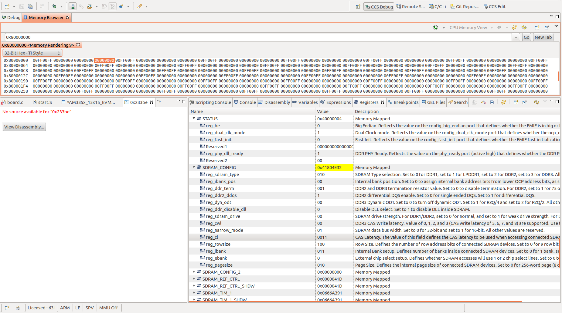
I am having issues getting DDR2 to talk on custom board using AM3352. The values cannot be read from DDR2. If I try to write to in the memory window of CCS, zeros are always returned.
Details
As a baseboard we were using AM335x EVM (TMDXEVM3358) which has two MT47H256M8 DDR parts. DDR2 on EVM worked fine. It's settings were
#define MT47H128M16RT25E_EMIF_READ_LATENCY 0x100005
#define MT47H128M16RT25E_EMIF_TIM1 0x0666B3C9
#define MT47H128M16RT25E_EMIF_TIM2 0x243631CA
#define MT47H128M16RT25E_EMIF_TIM3 0x0000033F
#define MT47H128M16RT25E_EMIF_SDCFG 0x41805332
#define MT47H128M16RT25E_EMIF_SDREF 0x0000081a
#define MT47H128M16RT25E_DLL_LOCK_DIFF 0x0
#define MT47H128M16RT25E_RATIO 0x80
#define MT47H128M16RT25E_INVERT_CLKOUT 0x00
#define MT47H128M16RT25E_RD_DQS 0x12
#define MT47H128M16RT25E_WR_DQS 0x00
#define MT47H128M16RT25E_PHY_WRLVL 0x00
#define MT47H128M16RT25E_PHY_GATELVL 0x00
#define MT47H128M16RT25E_PHY_WR_DATA 0x40
#define MT47H128M16RT25E_PHY_FIFO_WE 0x80
#define MT47H128M16RT25E_PHY_RANK0_DELAY 0x1
#define MT47H128M16RT25E_IOCTRL_VALUE 0x18B
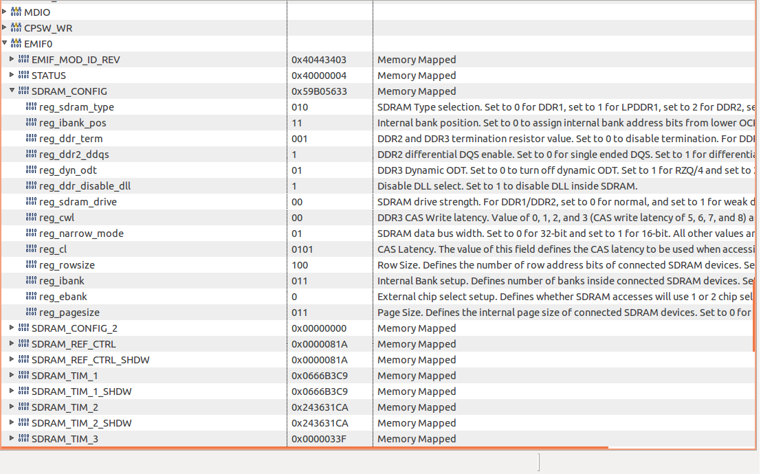
We have one MT47H64M16HR-25EITH part. The only changes in the configuration settings were
1) reg_rowsize field in SDRAM_CONFIG register was changed to 4 to represent 13 rows because the part has
64M x 16 has 13 rows, 10 columns and 8 banks x 16
2) reg_ibank_pos field was changed to 3 to allow 13 rows, 8 columns and 8 banks as shown in section 7.3.3.4.4 of reference manual SPRUH73J.
3) DDR2 PHY registers were configured according to the excel spreadsheet on http://processors.wiki.ti.com/index.php/AM335x_EMIF_Configuration_tips#Setting_Refresh_rate
with DDR_CK trace set to 1.312 and 1.312 for both bytes
DDR_DQSx set to 1.1162 for byte 0 and 1.137 for byte 1
PHY_INVERT_CLKOUT is set to 0
This resulted in
#define MT47H64M16HR25EITH_RD_DQS 0x40
#define MT47H64M16HR25EITH_PHY_FIFO_WE 0x6B
#define MT47H64M16HR25EITH_WR_DQS 0x2
#define MT47H64M16HR25EITH_PHY_WR_DATA 0x40
#define MT47H64M16HR25EITH_RATIO 0x80
4) I have also tried changing the refresh rate from 2074 to 1010.
5) The voltages to the DDR2 chip were verified. The layout was done as carefully as possible according to the suggestions.
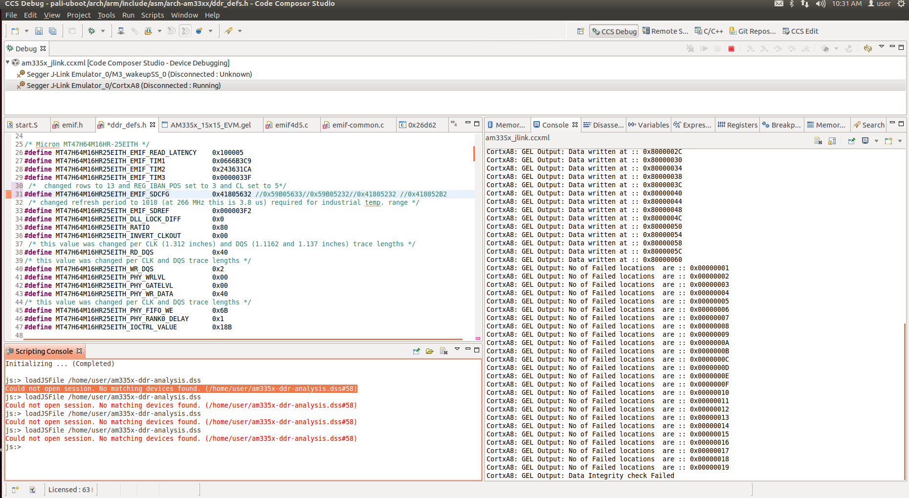
6) I see DDR clk, WE, CS, data and address lines on the scope. I see the data changing polarity when it try to write 1 or 0. However I suspect that when the data is read back it is always zero.
7) I have tried to apply the exact EVM settings without any improvement.
8) I did not modify any SPL boot sequence steps except for the pin-mux configuration changes so I do not think that it is a sequencing issue.
9) I have compares the timing registers (SDRAM_TIM1, SDRAM_TIM2 and SDRAM_TIM3) between our DDR2 and the DDR2 on the EVM and they appear to be the same.
Thanks
Oleg