This thread has been locked.

If you have a related question, please click the "Ask a related question" button in the top right corner. The newly created question will be automatically linked to this question.

DRA76P: JTAG EMU0/EMU1 connection

Part Number: DRA76P

Dear Expert.

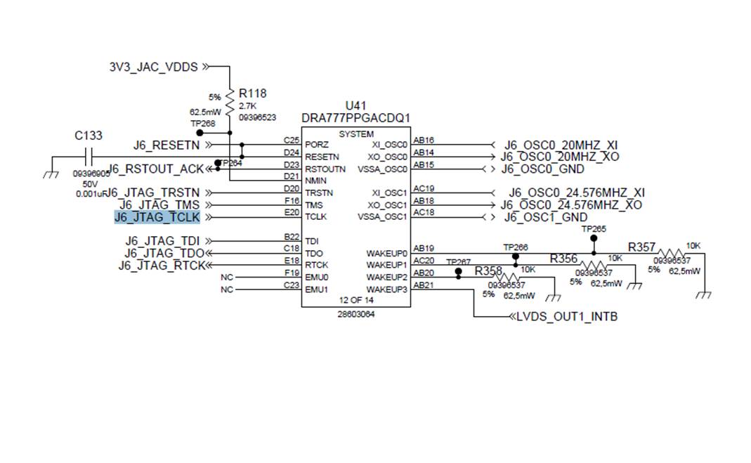
I wants to ask if emu0/emu1 is necessary to connect between emulator and Soc.

Our customer try to use TI 14-pin JTAG connector, but let emu0/emu1 unconnected.

when they using XDS560V2 STM emulator+CCS8.1 to debug on their board, they found that they can do "Test connection" action successfully. But they can not connect to MPU.

as TRM shown, emu0/emu1 should be pull up when debug.

Would you please help me to check if emu0/emu1 must be pull up with external resistor? Is there any way to solve this problem without making new board?

Thanks a lot!

yong

  • Supplemantary information, schematic :

      of JTAG part.

  • Yong, these pins are already pulled up internally at reset, see CTRL_CORE_PAD_EMU0 and CTRL_CORE_PAD_EMU1 registers. What error message do they get when trying to connect to the MPU? Are the gel scripts initializing the core successfully? 

    thanks

    Alex

  • Yong,

    Reminder, did you manage to solve your issue? If not can you send me the error message.

    thanks,
    Alex
  • Dear Alex.

    I've pushed customer to provide the error messages. Would you please hold this issue? I will update as soon as I get the feedback from customer.

    Thanks a lot!
    yong
  • Yong,

    No problem, post whenever you get feedback. If this thread gets locked due to several day timeout, just create a new one.

    thanks
    Alex
  • Dear Expert.

    We got the update from customer.

    When try to connect to MPU0 on customer board with emulator XDS560 STM, it shows.

    Cortex_M4_IPU1_C0: GEL Output: --->>> DRA7xxP Cortex M4 Startup Sequence In Progress... <<<---

    Cortex_M4_IPU1_C0: GEL Output: --->>> DRA7xxP Cortex M4 Startup Sequence DONE! <<<---

    Cortex_M4_IPU1_C1: GEL Output: --->>> DRA7xxP Cortex M4 Startup Sequence In Progress... <<<---

    Cortex_M4_IPU1_C1: GEL Output: --->>> DRA7xxP Cortex M4 Startup Sequence DONE! <<<---

    Cortex_M4_IPU2_C0: GEL Output: --->>> DRA7xxP Cortex M4 Startup Sequence In Progress... <<<---

    Cortex_M4_IPU2_C0: GEL Output: --->>> DRA7xxP Cortex M4 Startup Sequence DONE! <<<---

    Cortex_M4_IPU2_C1: GEL Output: --->>> DRA7xxP Cortex M4 Startup Sequence In Progress... <<<---

    Cortex_M4_IPU2_C1: GEL Output: --->>> DRA7xxP Cortex M4 Startup Sequence DONE! <<<---

    C66xx_DSP1: GEL Output: --->>> DRA7xxP C66x DSP Startup Sequence In Progress... <<<---

    C66xx_DSP1: GEL Output: --->>> DRA7xxP C66x DSP Startup Sequence DONE! <<<---

    C66xx_DSP2: GEL Output: --->>> DRA7xxP C66x DSP Startup Sequence In Progress... <<<---

    C66xx_DSP2: GEL Output: --->>> DRA7xxP C66x DSP Startup Sequence DONE! <<<---

    CortexA15_0: GEL Output: --->>> DRA7xxP Cortex A15 Startup Sequence In Progress... <<<---

    CortexA15_0: GEL Output: --->>> DRA7xxP Cortex A15 Startup Sequence DONE! <<<---

    CortexA15_1: GEL Output: --->>> DRA7xxP Cortex A15 Startup Sequence In Progress... <<<---

    CortexA15_1: GEL Output: --->>> DRA7xxP Cortex A15 Startup Sequence DONE! <<<---

    ARP32_EVE_1: GEL Output: --->>> Configuring EVE Memory Map <<<---

    ARP32_EVE_1: GEL Output: --->>> EVE Memory Map Done! <<<---

    ARP32_EVE_2: GEL Output: --->>> Configuring EVE Memory Map <<<---

    ARP32_EVE_2: GEL Output: --->>> EVE Memory Map Done! <<<---

    IcePick_D: GEL Output: Ipu RTOS is released from Wait-In-Reset.

    IcePick_D: GEL Output: Ipu SIMCOP is released from Wait-In-Reset.

    IcePick_D: GEL Output: IVAHD C66 is released from Wait-In-Reset.

    IcePick_D: GEL Output: IVAHD ICONT1 is released from Wait-In-Reset.

    IcePick_D: GEL Output: IVAHD ICONT2 is released from Wait-In-Reset.

    CS_DAP_DebugSS: GEL Output: --->>> CONFIGURE DEBUG DPLL settings to 1.9 GHZs  <<<---

    CS_DAP_DebugSS: GEL Output: > Setup DebugSS 1.9GHz in progress...

    CS_DAP_DebugSS: GEL Output: < Done with Setup DebugSS Trace export clock (TPIU) to 97MHz

    CS_DAP_DebugSS: GEL Output: < Done with Setup DebugSS PLL Clocking 1.9GHz

    CS_DAP_DebugSS: GEL Output: < Done with Setup DebugSS ATB Clocking 380MHz

    CS_DAP_DebugSS: GEL Output: < Done with Setup DebugSS Trace export clock (TPIU) to 97MHz

    CS_DAP_DebugSS: GEL Output: --->>> TURNING ON L3_INSTR and L3_3 clocks required for debug instrumention <<<<<<----

    CS_DAP_DebugSS: GEL Output: ---<<< L3 instrumentation clocks are enabled >>>> ---

    CS_DAP_DebugSS: GEL Output: --->>> Mapping TIMER supsend sources to default cores <<<<<<----

    CS_DAP_PC: GEL Output: Cortex-A15 1 is not in WIR mode so nothing to do.

    CortexA15_0: GEL Output: --->>> DRA7xxP Target Connect Sequence Begins ... <<<---

    CortexA15_0: GEL: Error while executing OnTargetConnect(): Target failed to read 0x4AE0C204

           at (*((unsigned int *) 0x4AE0C204)&0xF0000000) [DRA7xxP_startup_common.gel:138]

           at DRA7xxP_show_device_info() [DRA7xxP_startup_common.gel:116]

           at DRA7xxP_target_connect_sequence() [DRA7xxP_startup_common.gel:30]

           at OnTargetConnect()

    And also try to do "Test connection" action before that, the log shows.


    [Start: Spectrum Digital XDS560V2 STM USB Emulator_0]


    Execute the command:


    %ccs_base%/common/uscif/dbgjtag.exe -f %boarddatafile% -rv -o -F inform,logfile=yes -S pathlength -S integrity


    [Result]


    -----[Print the board config pathname(s)]------------------------------------


    C:\Users\vzksgm\AppData\Local\TEXASI~1\CCS\

        ti\0\0\BrdDat\testBoard.dat


    -----[Print the reset-command software log-file]-----------------------------


    This utility has selected a 560/2xx-class product.

    This utility will load the program 'sd560v2u.out'.

    Loaded FPGA Image: C:\ti\ccsv8\ccs_base\common\uscif\dtc_top.jbc

    The library build date was 'May 30 2018'.

    The library build time was '22:02:11'.

    The library package version is '8.0.27.9'.

    The library component version is '35.35.0.0'.

    The controller does not use a programmable FPGA.

    The controller has a version number of '6' (0x00000006).

    The controller has an insertion length of '0' (0x00000000).

    The cable+pod has a version number of '8' (0x00000008).

    The cable+pod has a capability number of '7423' (0x00001cff).

    This utility will attempt to reset the controller.

    This utility has successfully reset the controller.


    -----[Print the reset-command hardware log-file]-----------------------------


    The scan-path will be reset by toggling the JTAG TRST signal.

    The controller is the Nano-TBC VHDL.

    The link is a 560-class second-generation-560 cable.

    The software is configured for Nano-TBC VHDL features.

    The controller will be software reset via its registers.

    The controller has a logic ONE on its EMU[0] input pin.

    The controller has a logic ONE on its EMU[1] input pin.

    The controller will use falling-edge timing on output pins.

    The controller cannot control the timing on input pins.

    The scan-path link-delay has been set to exactly '2' (0x0002).

    The utility logic has not previously detected a power-loss.

    The utility logic is not currently detecting a power-loss.

    Loaded FPGA Image: C:\ti\ccsv8\ccs_base\common\uscif\dtc_top.jbc


    -----[The log-file for the JTAG TCLK output generated from the PLL]----------


      Test  Size   Coord      MHz    Flag  Result       Description

      ~~~~  ~~~~  ~~~~~~~  ~~~~~~~~  ~~~~  ~~~~~~~~~~~  ~~~~~~~~~~~~~~~~~~~

        1   none  - 01 00  500.0kHz   -    similar      isit internal clock

        2   none  - 01 09  570.3kHz   -    similar      isit internal clock

        3     64  - 01 00  500.0kHz   O    good value   measure path length

        4     16  - 01 00  500.0kHz   O    good value   auto step initial

        5     16  - 01 0D  601.6kHz   O    good value   auto step delta

        6     16  - 01 1C  718.8kHz   O    good value   auto step delta

        7     16  - 01 2E  859.4kHz   O    good value   auto step delta

        8     16  + 00 02  1.031MHz   O    good value   auto step delta

        9     16  + 00 0F  1.234MHz   O    good value   auto step delta

       10     16  + 00 1F  1.484MHz   O    good value   auto step delta

       11     16  + 00 32  1.781MHz   O    good value   auto step delta

       12     16  + 01 04  2.125MHz   O    good value   auto step delta

       13     16  + 01 11  2.531MHz   O    good value   auto step delta

       14     16  + 01 21  3.031MHz   O    good value   auto step delta

       15     16  + 01 34  3.625MHz   O    good value   auto step delta

       16     16  + 02 05  4.313MHz   O    good value   auto step delta

       17     16  + 02 13  5.188MHz   O    good value   auto step delta

       18     16  + 02 23  6.188MHz   O    good value   auto step delta

       19     16  + 02 37  7.438MHz   O    good value   auto step delta

       20     16  + 03 07  8.875MHz   O    good value   auto step delta

       21     16  + 03 15  10.63MHz   O    good value   auto step delta

       22     16  + 03 26  12.75MHz  {i}   stuck ir     auto step delta

       23     64  + 03 06  8.750MHz   i    stuck ir     auto power initial

       24     64  + 02 36  7.375MHz   O    good value   auto power delta

       25     64  + 02 3E  7.875MHz   O    good value   auto power delta

       26     64  + 03 02  8.250MHz   O    good value   auto power delta

       27     64  + 03 04  8.500MHz   O    good value   auto power delta

       28     64  + 03 05  8.625MHz   O    good value   auto power delta

       29     64  + 03 05  8.625MHz   O    good value   auto power delta

       30     64  + 02 3C  7.750MHz  {O}   good value   auto margin initial


    The first internal/external clock test resuts are:

    The expect frequency was 500000Hz.

    The actual frequency was 499110Hz.

    The delta frequency was 890Hz.


    The second internal/external clock test resuts are:

    The expect frequency was 570312Hz.

    The actual frequency was 569214Hz.

    The delta frequency was 1098Hz.


    In the scan-path tests:

    The test length was 2048 bits.

    The JTAG IR length was 6 bits.

    The JTAG DR length was 1 bits.


    The IR/DR scan-path tests used 30 frequencies.

    The IR/DR scan-path tests used 500.0kHz as the initial frequency.

    The IR/DR scan-path tests used 12.75MHz as the highest frequency.

    The IR/DR scan-path tests used 7.750MHz as the final frequency.


    -----[Measure the source and frequency of the final JTAG TCLKR input]--------


    The frequency of the JTAG TCLKR input is measured as 7.740MHz.


    The frequency of the JTAG TCLKR input and TCLKO output signals are similar.

    The target system likely uses the TCLKO output from the emulator PLL.


    -----[Perform the standard path-length test on the JTAG IR and DR]-----------


    This path-length test uses blocks of 64 32-bit words.


    The test for the JTAG IR instruction path-length succeeded.

    The JTAG IR instruction path-length is 6 bits.


    The test for the JTAG DR bypass path-length succeeded.

    The JTAG DR bypass path-length is 1 bits.


    -----[Perform the Integrity scan-test on the JTAG IR]------------------------


    This test will use blocks of 64 32-bit words.

    This test will be applied just once.


    Do a test using 0xFFFFFFFF.

    Scan tests: 1, skipped: 0, failed: 0

    Do a test using 0x00000000.

    Scan tests: 2, skipped: 0, failed: 0

    Do a test using 0xFE03E0E2.

    Scan tests: 3, skipped: 0, failed: 0

    Do a test using 0x01FC1F1D.

    Scan tests: 4, skipped: 0, failed: 0

    Do a test using 0x5533CCAA.

    Scan tests: 5, skipped: 0, failed: 0

    Do a test using 0xAACC3355.

    Scan tests: 6, skipped: 0, failed: 0

    All of the values were scanned correctly.


    The JTAG IR Integrity scan-test has succeeded.


    -----[Perform the Integrity scan-test on the JTAG DR]------------------------


    This test will use blocks of 64 32-bit words.

    This test will be applied just once.


    Do a test using 0xFFFFFFFF.

    Scan tests: 1, skipped: 0, failed: 0

    Do a test using 0x00000000.

    Scan tests: 2, skipped: 0, failed: 0

    Do a test using 0xFE03E0E2.

    Scan tests: 3, skipped: 0, failed: 0

    Do a test using 0x01FC1F1D.

    Scan tests: 4, skipped: 0, failed: 0

    Do a test using 0x5533CCAA.

    Scan tests: 5, skipped: 0, failed: 0

    Do a test using 0xAACC3355.

    Scan tests: 6, skipped: 0, failed: 0

    All of the values were scanned correctly.


    The JTAG DR Integrity scan-test has succeeded.


    [End: Spectrum Digital XDS560V2 STM USB Emulator_0]

    Thanks a lot

    yong

  • Hello,

    Thanks for providing the log results. Looks like the connection stress test passes fine. However the gels are crasing not able to read a device ID register.

    1. Are you booting an OS while trying to JTAG connect?
    2. Can you make sure you are using the latest device support package? processors.wiki.ti.com/.../Device_support_files

    thanks,
    Alex
  • Hello Yong,

    It's been a few days, can you answer my questions, let's solve this issues. Or if you already fixed it, please mark this thread done.

    thanks,

    Alex