


Hi everyone,
I have two question about OSC0.
(Q1) When LVCMOS square wave digital clock source is connected to OSC0, how should we design XTALOUT?
I have read the following sentences of DS. Is the XTALOUT pin NC acceptable?
Please let me know if there is a recommended circuit.
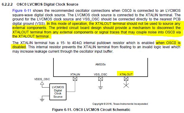
(Q2) Although it is described as "when OSC0 is disabled" in the above DS, is it to be disable by register?
Or is it disabled when an incorrect clock is input to XTALIN or when it is NC?
Best regards,
Sasaki

