This thread has been locked.

If you have a related question, please click the "Ask a related question" button in the top right corner. The newly created question will be automatically linked to this question.

AM3352: ADC input behavior

Part Number: AM3352

Hi.

My customer is investigating the behavior of an ADC errata (Advisory 1.0.32).
The power supply +5V is input to the PMIC, and the input of the ADC (AIN0) is open. The VDDA_ADC inputs the 1.8V output of the PMIC via a ferrite bead.

The following figures show the waveform at power-up.
The voltage is applied to AIN0 when VDDA_ADC power supply is turned on and VDD_CORE is not turned on. Could this be due to errata?

In addition, when VDD_CORE power is supplied, the voltage is applied for a short period of time. What is the reason for this?

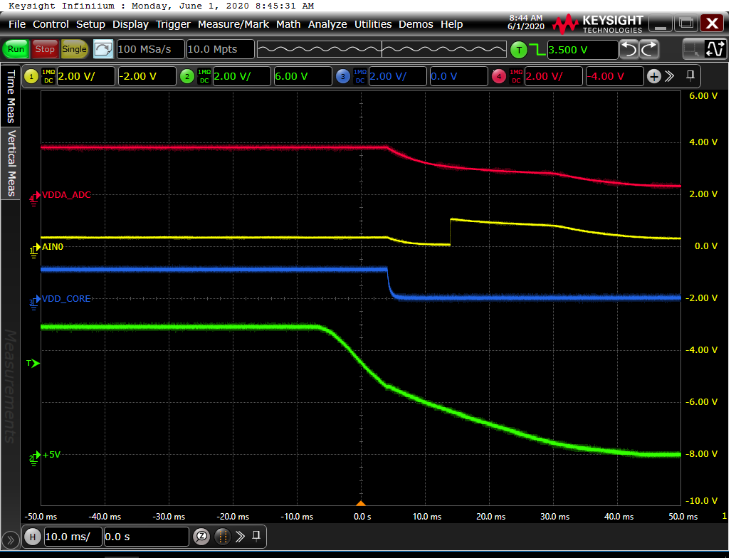
Also, The following figure shows the waveform at power down.
The voltage of VDDA_ADC appears at AIN0 about 10ms after VDDA_CORE falls, what is the reason for this?

Please tell me the reason for these behaviors and whether this is the assumed behavior.

Best Regards,
H.U

  • The observed condition and cause is described in the advisory, where the state of ADC input pins are not defined until all device power pins are valid after power-up. A similar thing can occur when power is turned off as the supplies ramp-down.

    Power supply decay after power has been turned off may take longer than power supplies ramp-up when power is turned on.  So these unexpected conditions may last longer as the supplies slowly ramp-down. The PWRONRSTn pin should be held low while the supplies ramp up and down to minimize these conditions.

    It is not clear what you need to know that has not already been described in the advisory.

    Regards,
    Paul