This thread has been locked.

If you have a related question, please click the "Ask a related question" button in the top right corner. The newly created question will be automatically linked to this question.

AM3354: About the ADC Specifications

Part Number: AM3354

Hi,

I have questions about ADC of AM335x.


Q1:I have heard before in the following thread that ADC does not have a discharge circuit.
      However, even without the intended discharge circuit, I think the sampling capacitor is discharging a little due to the tiny leakage current.
      I think the timing of this small amount of discharge is between the end of AD conversion and one clock cycle after the start of sampling. Is this correct?

<<about the ADC errata : Advisory 1.0.32>>

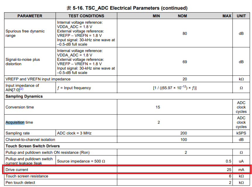
Q2:If the ADC terminal is shorted to VSS_ADC, do I need to take care of the incoming current as well? Or is it okay if it is less than 25mA as specified in the datasheet?


Q3:What is the maximum value of the outflow current when this errata phenomenon occurs?
      Also, am I correct in understanding that the maximum value limit of the income current is 25mA?


Best Regards,
UNA

  • Hi UNA,

    To answer your questions in order:

    1. The capacitor will have some residual charge that remains from the conversion and will need to be recharged during the next acquisition. Since the next acquisition may or may not occur immediately after the conversion depending on ADC configuration, you should assume that the residual charge will be anywhere between VSS and VDD, so the source impedance needs to be able to fully charge the capacitor no matter what the initial residual charge is when acquisition begins. 

    The small discharge you are talking about results from internal leakage of both the capacitor as well as the path from the input pin to the internal analog multiplexer that feeds the capacitor. 

    2. There is no specific limitation on the AM335x side, the advisory is targeted mainly at potential internal shorts that can/will occur and ways in which you should protect the source device. You need to understand the limitations of the attached devices and apply the appropriate series resistors to protect them. The caveat here being that you also need to understand the effect a series resistor can have when you consider input leakage and time required to charge the sampling capacitor during the acquisition period. If the input is not used, the errata defines a specific resistor value to VSS that should be used to protect the device

    3. You should assume that the maximum outflow current is infinite and do what is necessary to protect the attached device. Once again, for unused pins they should be connected using the recommended-size pull-down resistor to VSS. 

    Best Regards,

    Andrei

  • Hi Andrei,

    Thank you for your reply.

    I understood that the outflow current must be assumed to be infinite, However does the maximum value limit of the inflow current when this problem occurs should not exceed 25mA, as shown in  the DS below?

    Best Regards,
    UNA

  • Hi UNA,

    That parameter is saying that the Touch Screen Switch Drivers attached on the ADC are able to source up to 25mA into the device attached to the ADC, the expected device being a resistive touchscreen. So yes it should not exceed that value. 

    Best Regards,

    Andrei

  • Hi Andrei,

    The Drive current is the maximum current that can be output from the AIN pin?
    So what is the maximum current that can be input to the AIN terminal?

    Best Regards,
    UNA

  • Hi UNA,

    There is no "safe" maximum input current that is defined for what can be input to the device AIN terminals. This is because under normal circumstances (in devices that are not susceptible to the errata), this should never be an issue. What the errata tries to explain, is that because of the internal muxing logic of the device, it is possible that the ADC pins are briefly taken to an unknown state during boot that can be anywhere from VSS to VDD, as such the source could be briefly "shorted" to ground for example.

    Normally we do not expect that this will cause any damage to our device, but, out of an abundance of caution, we advise on the use of a series resistor of 500 Ohms (as defined in the errata) mainly as a precaution for the source device from being overloaded during the bootup sequence.  

    As for the max current that can be sourced by the AIN pin in that mode, because of the internal layout the pin is likely able to source much more current, but 25mA should be seen as the reference of what it can provide as defined by the datasheet. 

    Best Regards,

    Andrei