

Part Number: 66AK2E05
Hi,
How to calculate the "DDR3 Interface – Registers" for Keystone II devices and Test/Debug on Keystone II EVM ?

This thread has been locked.
If you have a related question, please click the "Ask a related question" button in the top right corner. The newly created question will be automatically linked to this question.
Part Number: 66AK2E05
Hi,
How to calculate the "DDR3 Interface – Registers" for Keystone II devices and Test/Debug on Keystone II EVM ?
DDR3 Interface – Register calculation for Keystone II devices and Test/Debug on Keystone II EVM.
Documents to read at first sight:
Pre-requisite:
[ For examples DDR3 Memories from Micron, Samsung etc.
The user may select the memories from any brands; However, here, let us take
MT41K512M16 with speed grade 1600 MTS from Micron. So, download the appropriate datasheet from the micron website, like below.
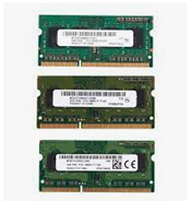
Sample parts to know how the DDR3 memories will-look-like
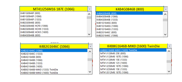
List of DDR3 Memories for which the register values are already calculated .
Sequence:
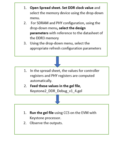
If DDR3 memory is one among the list, follow the procedure below
|
SDRAM and PHY Configuration |
|
|
Register |
|
|
DDR_TERM |
RZQ/4 |
|
DYN_ODT |
Disable ODT |
|
SDRAM_DRIVE |
RZQ/7 |
|
CAS_WRITE_LATENCY |
CWL = 8 |
|
Narrow Mode |
64-bit bus width |
|
ECC Byte |
Enable |
|
CAS_LATENCY |
CAS = 11 |
|
IBANK |
8 bank SDRAM |
|
EBANK |
Single Rank - only use CE0 |
|
PAGESIZE |
1024-word page - 10 column bits |
|
ADDRESS_MIRRORING |
Address Mirroring Off |
|
PHY Data ZO |
RZQ/6 = 40 Ohms |
|
PHY ACCC ZO |
RZQ/7 = 34 Ohms |
|
PHY ODT |
RZQ/4 = 60 Ohms |
|
DDR3 or DDR3L |
DDR3 |
|
Refresh Configuration |
|
|
Selected |
|
|
INITREF_DIS |
Normal Operation |
|
SRT |
Extended Temp Range |
|
ASR |
Manual Self-Refresh |
|
PASR |
Full Array |
|
REFRESH_PERIOD - Normal |
7.81 |
|
REFRESH_PERIOD - Ext. Temp |
3.91 |
|
EMIF Configuration Register Values |
||
|
SDRAM Register |
Address (hex) |
Value (hex) |
|
DDR_SDTIM1 |
21010018 |
2EDD34FB |
|
DDR_SDTIM2 |
2101001C |
00001EB5 |
|
DDR_SDTIM3 |
21010020 |
96BDFFB7 |
|
DDR_SDTIM4 |
21010028 |
587F19FF |
|
DDR_SDCFG |
21010008 |
6200CE62 |
|
DDR_SDRFC (normal) |
21010010 |
000030D3 |
|
DDR_SDRFC |
21010010 |
00001869 |
|
DDR_ZQCFG |
210100C8 |
70073200 |
|
PHY Configuration Register Values |
||
|
SDRAM PHY Register |
Address (hex) |
Value (hex) |
|
DDR3_PGCR0 |
02329008 |
A8000E3F |
|
DDR3_PGCR1 |
0232900C |
0080C487 |
|
DDR3_PGCR2 |
0232908C |
00F07A12 |
|
DDR3_PLLCR |
02329018 |
0001C000 |
|
DDR3_MR0 |
02329054 |
00001C70 |
|
DDR3_MR1 |
02329058 |
00000006 |
|
DDR3_MR2 |
0232905C |
00000098 |
|
DDR3_MR3 |
02329060 |
00000000 |
|
DDR3_DTPR0 |
02329048 |
9D9CBB66 |
|
DDR3_DTPR1 |
0232904C |
32868400 |
|
DDR3_DTPR2 |
02329050 |
5002D200 |
|
DDR3_PTR0 |
0232901C |
42C21590 |
|
DDR3_PTR1 |
02329020 |
D05612C0 |
|
DDR3_PTR2 |
02329024 |
00083DEF |
|
DDR3_PTR3 |
02329028 |
0D861A80 |
|
DDR3_PTR4 |
0232902C |
0C827100 |
|
DDR3_DCR |
02329044 |
0000040B |
|
DDR3_DTCR |
02329068 |
710035C7 |
|
DDR3_ZQ0CR1 |
02329184 |
0001005D |
|
DDR3_ZQ1CR1 |
02329194 |
0001005B |
|
DDR3_ZQ2CR1 |
023291A4 |
0001005B |
|
DDR3_DX2GCR |
02329240 |
7C000E81 |
|
DDR3_DX3GCR |
02329280 |
7C000E81 |
|
DDR3_DX4GCR |
023292C0 |
7C000E81 |
|
DDR3_DX5GCR |
02329300 |
7C000E81 |
|
DDR3_DX6GCR |
02329340 |
7C000E81 |
|
DDR3_DX7GCR |
02329380 |
7C000E81 |
|
DDR3_DX8GCR |
023293C0 |
7C000E81 |
If new to run the gel file on the EVM, follow the procedure given at
If DDR3 memory is not in the list, follow the procedure below:
For example: Let us take the timing parameter, “ T_RP”, the value to be filled is 13.75 ns with reference to the datasheet of the memory device for its appropriate speed grade.
Similarly fill all the timing values.
|
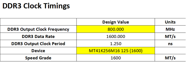
DDR3 Clock Timings |
||
|
Design Value |
Units |
|
|
DDR3 Output Clock Frequency |
800.000 |
MHz |
|
DDR3 Data Rate |
1600.000 |
MT/s |
|
DDR3 Output Clock Period |
1.250 |
ns |
|
Device |
User Defined |
|
|
Speed Grade |
1333 |
MT/s |
|
SDRAM and PHY Configuration |
|
|
Register |
|
|
DDR_TERM |
RZQ/4 |
|
DYN_ODT |
Disable ODT |
|
SDRAM_DRIVE |
RZQ/7 |
|
CAS_WRITE_LATENCY |
CWL = 8 |
|
Narrow Mode |
64-bit bus width |
|
ECC Byte |
Enable |
|
CAS_LATENCY |
CAS = 11 |
|
IBANK |
8 bank SDRAM |
|
EBANK |
Single Rank - only use CE0 |
|
PAGESIZE |
1024-word page - 10 column bits |
|
ADDRESS_MIRRORING |
Address Mirroring Off |
|
PHY Data ZO |
RZQ/6 = 40 Ohms |
|
PHY ACCC ZO |
RZQ/7 = 34 Ohms |
|
PHY ODT |
RZQ/4 = 60 Ohms |
|
DDR3 or DDR3L |
DDR3 |
|
Refresh Configuration |
|
|
Selected |
|
|
INITREF_DIS |
Normal Operation |
|
SRT |
Extended Temp Range |
|
ASR |
Manual Self-Refresh |
|
PASR |
Full Array |
|
REFRESH_PERIOD - Normal |
7.81 |
|
REFRESH_PERIOD - Ext. Temp |
3.91 |
|
EMIF Configuration Register Values |
||
|
SDRAM Register |
Address (hex) |
Value (hex) |
|
DDR_SDTIM1 |
21010018 |
166C9855 |
|
DDR_SDTIM2 |
2101001C |
00001D4A |
|
DDR_SDTIM3 |
21010020 |
421DFF54 |
|
DDR_SDTIM4 |
21010028 |
553F07FF |
|
DDR_SDCFG |
21010008 |
6200CE62 |
|
DDR_SDRFC (normal) |
21010010 |
00001869 |
|
DDR_SDRFC |
21010010 |
00000C34 |
|
DDR_ZQCFG |
210100C8 |
70073200 |
|
PHY Configuration Register Values |
||
|
SDRAM PHY Register |
Address (hex) |
Value (hex) |
|
DDR3_PGCR0 |
02329008 |
A8000E3F |
|
DDR3_PGCR1 |
0232900C |
0080C487 |
|
DDR3_PGCR2 |
0232908C |
00F07A12 |
|
DDR3_PLLCR |
02329018 |
0001C000 |
|
DDR3_MR0 |
02329054 |
00001C70 |
|
DDR3_MR1 |
02329058 |
00000006 |
|
DDR3_MR2 |
0232905C |
00000098 |
|
DDR3_MR3 |
02329060 |
00000000 |
|
DDR3_DTPR0 |
02329048 |
9D5CBB66 |
|
DDR3_DTPR1 |
0232904C |
32840300 |
|
DDR3_DTPR2 |
02329050 |
50035200 |
|
DDR3_PTR0 |
0232901C |
42C21590 |
|
DDR3_PTR1 |
02329020 |
D05612C0 |
|
DDR3_PTR2 |
02329024 |
00083DEF |
|
DDR3_PTR3 |
02329028 |
08861A80 |
|
DDR3_PTR4 |
0232902C |
0C827100 |
|
DDR3_DCR |
02329044 |
0000040B |
|
DDR3_DTCR |
02329068 |
710035C7 |
|
DDR3_ZQ0CR1 |
02329184 |
0001005D |
|
DDR3_ZQ1CR1 |
02329194 |
0001005B |
|
DDR3_ZQ2CR1 |
023291A4 |
0001005B |
|
DDR3_DX2GCR |
02329240 |
7C000E81 |
|
DDR3_DX3GCR |
02329280 |
7C000E81 |
|
DDR3_DX4GCR |
023292C0 |
7C000E81 |
|
DDR3_DX5GCR |
02329300 |
7C000E81 |
|
DDR3_DX6GCR |
02329340 |
7C000E81 |
|
DDR3_DX7GCR |
02329380 |
7C000E81 |
|
DDR3_DX8GCR |
023293C0 |
7C000E81 |
If new to run the gel file on the EVM, follow the procedure given at
---
Visit this FAQ on "DDR3 Read write test code" (or) How to do DDR3 test on C6678 EVM or K2H EVM board ?
Regards
Shankari G
