This thread has been locked.

If you have a related question, please click the "Ask a related question" button in the top right corner. The newly created question will be automatically linked to this question.

PCIe Performance vs. Payload size


I'm using the C6678 as a root complex. The DSP and a FPGA are connected to a PCIe switch. The FPGA is writing to DSP memory (posted writes) and I am trying to optimize performance.

The document SPRABK8 suggests, that the payload size can be increased from 128 bytes to 256 bytes for inbound transfers, which reduces the overhead.

The problem is, that the transmission gets slower if the the Maximum Payload Size value in the Device Capabilities Register is increased to 256 bytes without actually increasing the payload size. The performance further decreases if the payload size itself is increased.

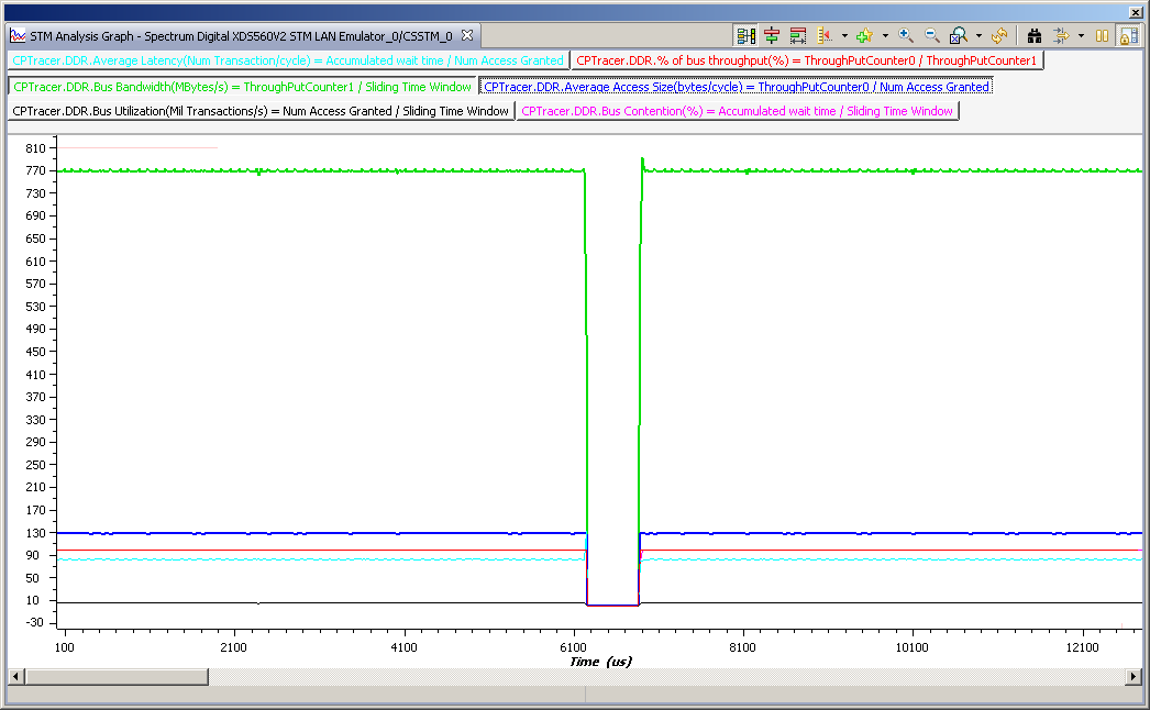
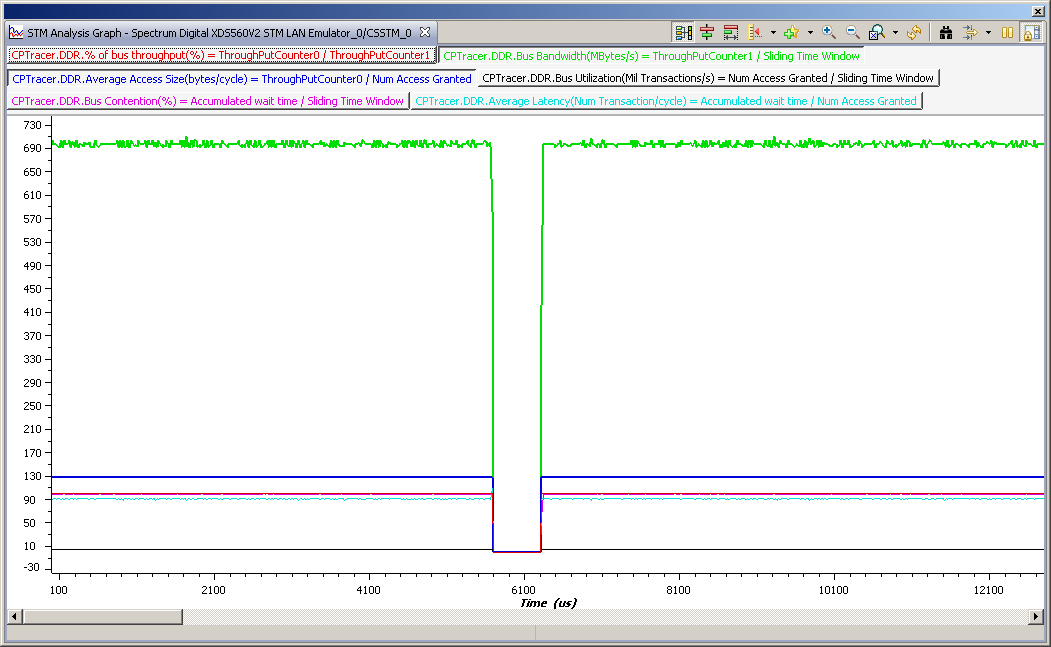
These are the results:

Maximum payload size
(Device capabilities)
Used payload size Data rate
128 64 717 MB/s
128 128 780 MB/s
256 64 717 MB/s
256 128 695 MB/s
256 256 530 MB/s

Any ideas?

Thanks,

Ralf

  • Ralf,

    Could you clarify which register has been programmed please?

    The MAX_PAYLD_SZ (bits[2:0]) in DEVICE_CAP register is normally a read-only field. It shows the maximum payload size that supported in the device. 000b=128 bytes and 001b=256 bytes.

    The MAX_PAYLD (bits[7:5]) in DEV_STAT_CTRL register could be programmed to set the max TLP data payload size. 000b=128 bytes and 001b=256 bytes. The permissible values that can be programmed are indicated by the MAX_PAYLD_SZ in DEVICE_CAP as mentioned above.

    Could you also check the actual payload size in the TLP of each scenario you are testing please? We should make sure the actual payload size in the TLP is indeed the values we programmed in the FPGA and received by DSP. Please check the TLP coming in and out of the PCIe Switch to make sure the Switch does not decrease the performance in each scenario. You may need protocol analyzer or something similar to verify the TLP.

    Sincerely,

    Steven

  • Hi Steven,

    I actually programmed bits[7:5] of the Device Control Register, sorry for the confusion.

    I already checked the payload sizes of the outgoing TLPs within the FPGA. I will also try to check the incoming TLP size using the System Trace.

    The strange thing is that the performance decreases for 128 byte TLPs, only by increasing the MAX_PAYLD value. The Switch and the FPGA don't know about this change.

    Thanks,

    Ralf

  • I did some tests with the XDS560v2 CP System Trace.

    Trace Settings:

    • Transaction Monitor: DDR3 (PCI write destination memory)
    • Function: Transaction Statistics
    • Bandwidth Type: Total Bandwidth Profile
    • Transaction Master: PCIe
    • Sample Window: 10000 (20us)

    Results:

    The most interesting signals are the bus bandwidth (green) and the access size (blue). There is a pause in data transmission for a few hundred us, which is normal.

    • MAX_PAYLD: 128 byte, Payload: 128 byte

    • MAX_PAYLD: 256 byte, Payload: 128 byte


    • MAX_PAYLD: 256 byte, Payload: 256 byte

    For 256 byte payload packets, the Average Access Size remains at 128 bytes (blue line). I'm not sure if the packets get divided by the DSPs PCIe unit.

    Maybe it's possible for someone to do a performance test with two Keystone devices connected to each other, like in sprabk5.pdf. The idea is to change the MAX_PAYLD register to 256 byte and to check if the throughput then decreases like in my case.

    Thanks,

    Ralf

  • Ralf,

    Thanks a lot for your testing in detail.

    We also did some analysis on KeyStone devices. If the PCIe max payload size is set as 256B (larger than 128B), there will be some idle cycles inserted on the bridge that affecting the throughput performance. So the maximum performance for PCIe throughput on KeyStone devices could only be achieved with payload size as 128B (the default setup).

    Thanks a lot for your response and your time. Hope the PCIe throughput with 128B could still meet your requirement.

    Sincerely,

    Steven

  • Hello Ralf , I felicitate your for successing the communication betwenn DSP and FPGA via the PCIE Switch ,

    We are doing the same thing but with two DSPs and we are facing problems ,

    Please can you tell me how was the configuration of your switch registers ? 

    did you use the LLD Driver and Ti Example of Pcie on the DSP .?

    thank you very much Ralf 

  • Hello,

    in our system, the DSP is the root complex which enumerates the PCI bus. This will setup the required registers of each PCI bridge inside the switch:

    • Bus Number Registers (Primary, Secondary, Subordinate)
    • Memory Base and Memory Limit Register
    • Enable memory space and bus master bits in the Command Register

    It also helps to evaluate error registers of the switch and the DSP if something is not working.

    I use the PCIe LLD for accessing registers (Pcie_readRegs(), Pcie_writeRegs()).

    Ralf

  • Hello,

    We have a similar question on PCIe throughput performance. Our DSP(C6678) is configured as RC and the FPGA as EP. They are directly connected to each other -no PCIe switch-. The MAX_PAYLD (bits[7:5]) is programmed to 000b as Steven pointed out. We get 720MB/s data rate for 64B payload which is close to value that Ralf suggests. However, for 128B payload, we could only achieve 695MB/s which should have been 780MB/s. In addition if we set MAX_PAYLD (bits[7:5]) to 001b, then we get more drastic reductions in the throughput. What might be missing here?

    Any suggestions?

    Thanks,

    Abdulkerim
  • Hi,

    Have you using EDMA to transmit data?
    when using EDMA to receive data from the Keystone PCIe, the transfer controller (TC) that is used should be taken into consideration. Not all transfer controllers use the same data burst size (DBS), and the size of the data burst can have an impact on the performance of the PCIe peripheral.

    For example, if an EDMA TC with a 64-byte data burst size is chosen, then the PCIe will use 64-byte payloads, and packet overhead will be introduced for every 64 bytes of payload data. Transferring 128 bytes using two 64-byte data payloads will introduce twice as much overhead as a one 128-byte data payload.

    Thanks,
  • Hi Ganapathi,

    Thanks for your answer.

    We don't use EDMA to transmit data. Instead, FPGA writes the data to DSP DDR3 memory via PCIe.

    By the way, we checked the related PCIe signals from the FPGA side. We observed that, in the 64B payload case, the FPGA is able to send the TLP's successively with very rarely occuring idle cycles - the cycles in which the remote device (DSP PCIESS)issues a NOT READY signal to the PCIe IP in the FPGA side and as a result the FPGA waits for the READY signal to transmit the next TLP-. However, in the 128B payload case, the so-called idle cylces appear very often and thus the decrease in the throughput becomes inevitable.

    Did we somehow misconfigured a register in the PCIESS which might result in such a degradation?

    Regards,

    Abdulkerim
  • Sorry for the delay...I am escalating this post...

  • Hi
    Can you please clarify the speed that you are running the device and DDR?
    The original post and throughput data was from Ralf , and I am not sure if these were internally replicated results in TI. The data that TI publishes is with DSP to DSP , with EDMA used for the burst etc.
    I didn't see Ralf's post have any info on the speed of operations , but it would be good to understand what speeds you are running at.

    Regards
    Mukul
  • Hi Mukul,

    Sorry for my late response.
    Interestingly I can not see your post here, I read your answer from the notification mail. But for completeness I put your answer below:

    --------------------------------------------------------------------------------------------------------------------------------------------------
    Mukul Bhatnagar replied to PCIe Performance vs. Payload size:

    Hi
    Can you please clarify the speed that you are running the device and DDR?
    The original post and throughput data was from Ralf , and I am not sure if these were internally replicated results in TI.
    The data that TI publishes is with DSP to DSP , with EDMA used for the burst etc.
    I didn't see Ralf's post have any info on the speed of operations , but it would be good to understand what speeds you are running at.

    Regards
    Mukul
    --------------------------------------------------------------------------------------------------------------------------------------------------

    Our device -the DSP- runs at 1GHz, the DDR3CLKOUT frequency is 666.667MHz so the data transfer speed is 1333MT/s.

    Thanks,
    Abdulkerim
  • Abdulkerim,

    There are two registers:

    offset 0x1074: DEVICE_CAP, bit 2-0 MAX_PAYLD_SZ Maximum Payload size supported, by default it is 001 (this is a read-only field, it is not expected to change).  

    000b 128 bytes max payload size

    001b 256 bytes max payload size

    offset 0x1078: DEV_STAT_CTRL, bit 7-5, MAX_PAYLD, by default it is 000 (can be programmed to 000 or 001, limited to the DEVICE_CAP MAX_PAYLD_SZ field).

    000b 128 bytes max payload size

    001b 256 bytes max payload size

    There is no other fields to control the max TLP payload size. As suggested by Steven, the MAX_PAYLD has to be programed to 000 for best throughput. In your cases, what if you change the DSP memory from DDR to other locations, say MSMC or L2? Will this make any difference using 64 bytes or 128 bytes payload size writing from FPGA?

    Regards, Eric

  • to avoid delays, please avoid posting questions on posts that are marked as "answered"....start a new post with new questions and make reference to related posts. Thanks Eric for replying this one.
  • Hi Eric,

    Please check and support new follow up thread from below link,

    Thank you.

  • Hello!

    Although its a very old thread, still I wish to put my contribution here.

    When it comes to EDMA+PCIe operation, things become more complicated. People think about EDMA3 Default Busrt Size (DBS) defined for each EDMA3 instance. I am practically confident, that DBS is not obeyed with EDMA3 initiated outbound transfers. On C6670 as RC with Spartan 6 FPGA as EP monitoring transaction interface I have found, that EDMA3 of DSP produces read requests for 128B, but issues posted writes of 64B payload even on EDMA3CC0 with DBS of 128B.

    TI people clearly stated they never monitored PCIe itself ASSUMING EDMA3 operates according to its spec. Instead they measured throughput, one may find numbers in sprabk8 PCIe Use Cases for KeyStone Devices. It was noticed, that read performance exceeds write performance without attempt to give an explanation. I think I have one. There is a thread about PCIe outbound payload size with EDMA with no answer at time of writing this message.