This thread has been locked.

If you have a related question, please click the "Ask a related question" button in the top right corner. The newly created question will be automatically linked to this question.

How to configure the MPUs on the OMAP-L138?

I'm trying to utilize the MPUs on the OMAP L138. I'm having trouble getting it to do anything.

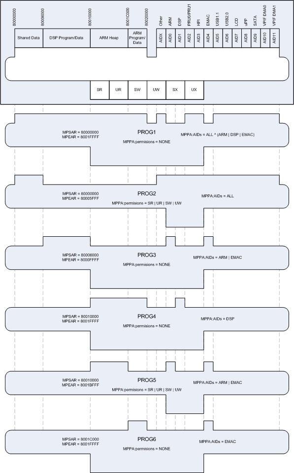
I'm trying to test MPU1 which serves the L3 shared RAM. MPU1 has 6 programmable ranges.

I'm running code on the ARM to configure and test MPU1. It's configuring 4 of the six ranges as follows:

Range # MPSAR (Start Address) MPEAR (End Address) MPPA MPPA->AIDs MPPA->Access Types
0 0x80000000 0x80002FFF 0x00000C36 ARM, DSP SR, SW, UR, UW
1 0x80003000 0x80005FFF 0x00000C36 ARM, DSP SR, SW, UR, UW
2 0x80006000 0x8000FFFF 0x0000083F DSP SR, SW, SX, UR, UW, UX
3 0x80010000 0x8001FFFF 0x0000043F ARM SR, SW, SX, UR, UW, UX

I've tried both leaving the remaining two ranges at their defaults of:

Range # MPSAR (Start Address) MPEAR (End Address) MPPA MPPA->AIDs MPPA->Access Types
4 0x80000000 0x8001FFFF 0x03FFFEBF All All
5 0x80000000 0x8001FFFF 0x03FFFEBF All All

And I've tried configuring the remaining two ranges as follows:

Range # MPSAR (Start Address) MPEAR (End Address) MPPA MPPA->AIDs MPPA->Access Types
4 0x80000000 0x8001FFFF 0x00000000 None None
5 0x80000000 0x8001FFFF 0x00000000 None None

After configuring the ranges in MPU1, the code then enables interrupts by setting the PROTERR_EN bit (bit 0) in IENSET of MPU1 and setting the PROTERR_EN bit (bit 0) in IENSET of SYSCFG0.

Then to test the protection, my code (running on the ARM) tries to write to 0x80006000, which I would expect the MPU to prevent. But, the MPU doesn't prevent the write, and it doesn't signal an interrupt and there is nothing in it's FLTSTAT and FLTADDR registers after this. It's as if the MPU isn't doing anything.

Is there some step I'm missing to enable the MPU?

I thought maybe running this test code with the debugger / emulator might be an issue, so I've tried running it booted from SPI FLASH, but the MPU still doesn't prevent the ARM from writing to that address.

Anyone have any insight?

Thanks,
Arthur

  • I have exactly similar problem as above. No matter what I do, the MPU fails to protect anything. As a test to verify some action from the MPU I have set the registers in MPU1 and MPU2 to disallow all access from all initiators at the full address space, that they cover. But even so, the Linux and DSP system boots and works as if nothing happend. 

    To verify that other parts of the Linux kernel or DSP code does not reconfigure the MPU, I have read out the register content with a JTAG after the system was fully booted. The register settings are exactly as I configured them but even so, the MPU's still does not work. Below is a register dump of the MPU1 and MPU2 register content. 

    Anyone have an idea? Could someone from TI please confirm that this module is in fact working?

    Any input would be appreciated.

    Thanks,

    Thomas

    N.B: I can provide a memory dump, but the E2E web site did not allow me to insert pictures or attachments. I will be happy to provide these memory dumps on your request.

  • Hi Arthur

    We regret the delay in responding to this issue. 

    Can you provide some more background on this issue

    1) What OS are you using?

    2) Can you confirm that when doing all of this configuration ARM is in supervisor mode (this might not be required, if you are seeing the desired values on the MPU registers)?

    3) Would it be possible for you to share your code snippets, actual register values for the programmed MPU registers etc. 

    4) Instead of selectively trying to protect some regions, and look at interrupt functionality, have you tried to lock down everything (say all memory regions from both ARM/DSP) and see if that helps generate the interrupts properly and/or bar accesses?

    Arthur James said:
    which I would expect the MPU to prevent. But, the MPU doesn't prevent the write, and it doesn't signal an interrupt and there is nothing in it's FLTSTAT and FLTADDR registers after this.

    One point of clarification for FLSTAT/FLTADDR registers etc that you see in MPUs and SYSCFG register memory map.  As far as I know these registers are only meant to catch faulty addresses when ARM or DSP tries to write to reserved locations within the memory map of these modules e.g . writes/accesses to 01E1 4028h to 01E1 40FCh in the MPU1 memory map will be registered as address errors, and show the access locations in FLTADDR etc.

    Regards

    Mukul 

  • Please find below a hexdump of the register content of MPU2. 3 regions are defined, and the rest of the regions are defined at the full memory area with no permissions and no allowed AID. The below setting should effectively protect the entire DDR2 area from ARM, DSP and any other initiators. However it seems to have no effect. The system continues to boots fine anyway. I configure the register settings during the boot of the Linux kernel in kernel mode and have read out the register contents with a JTAG after boot (and of course after disabling the MMU). I have also tried the same configuration in u-boot but with the same result. I can't seem to understand why the MPU2 apparently completely ignore my settings. 

    Could someone please comment, why this setting does not work, or what is wrong with this configuration? 

    Thanks and best regard,

    Thomas

    Register content from address 0x01E1:5000:

    0x4E814901 0x060CC001 0x00000000 0x00000000 0x00000000 0x00000000 0x00000000 0x00000000
    0x00000000 0x00000000 0x00000000 0x00000000 0x00000000 0x00000000 0x00000000 0x00000000
    0x00000000 0x00000000 0x00000000 0x00000000 0x00000000 0x00000000 0x00000000 0x00000000
    0x00000000 0x00000000 0x00000000 0x00000000 0x00000000 0x00000000 0x00000000 0x00000000
    0x00000000 0x00000000 0x00000000 0x00000000 0x00000000 0x00000000 0x00000000 0x00000000
    0x00000000 0x00000000 0x00000000 0x00000000 0x00000000 0x00000000 0x00000000 0x00000000
    0x00000000 0x00000000 0x00000000 0x00000000 0x00000000 0x00000000 0x00000000 0x00000000
    0x00000000 0x00000000 0x00000000 0x00000000 0x00000000 0x00000000 0x00000000 0x00000000
    0x00000000 0x00000000 0x00000000 0x00000000 0x00000000 0x00000000 0x00000000 0x00000000
    0x00000000 0x00000000 0x00000000 0x00000000 0x00000000 0x00000000 0x00000000 0x00000000
    0x00000000 0x00000000 0x00000000 0x00000000 0x00000000 0x00000000 0x00000000 0x00000000
    0x00000000 0x00000000 0x00000000 0x00000000 0x00000000 0x00000000 0x00000000 0x00000000
    0x00000000 0x00000000 0x00000000 0x00000000 0x00000000 0x00000000 0x00000000 0x00000000
    0x00000000 0x00000000 0x00000000 0x00000000 0x00000000 0x00000000 0x00000000 0x00000000
    0x00000000 0x00000000 0x00000000 0x00000000 0x00000000 0x00000000 0x00000000 0x00000000
    0x00000000 0x00000000 0x00000000 0x00000000 0x00000000 0x00000000 0x00000000 0x00000000
    0xC0000000 0xC5FFFFFF 0x000000C0 0x00000000 0xC6000000 0xC7FFFFFF 0x000000C0 0x00000000
    0xC8000000 0xDFFFFFFF 0x000000C0 0x00000000 0xC0000000 0xDFFFFFFF 0x000000C0 0x00000000
    0xC0000000 0xDFFFFFFF 0x000000C0 0x00000000 0xC0000000 0xDFFFFFFF 0x000000C0 0x00000000
    0xC0000000 0xDFFFFFFF 0x000000C0 0x00000000 0xC0000000 0xDFFFFFFF 0x000000C0 0x00000000
    0xC0000000 0xDFFFFFFF 0x000000C0 0x00000000 0xC0000000 0xDFFFFFFF 0x000000C0 0x00000000
    0xC0000000 0xDFFFFFFF 0x000000C0 0x00000000 0xC0000000 0xDFFFFFFF 0x000000C0 0x00000000
    0x00000000 0x00000000 0x00000000 0x00000000 0x00000000 0x00000000 0x00000000 0x00000000
    0x00000000 0x00000000 0x00000000 0x00000000 0x00000000 0x00000000 0x00000000 0x00000000
    0x00000000 0x00000000 0x00000000 0x00000000 0x00000000 0x00000000 0x00000000 0x00000000
    0x00000000 0x00000000 0x00000000 0x00000000 0x00000000 0x00000000 0x00000000 0x00000000
    0x00000000 0x00000000 0x00000000 0x00000000 0x00000000 0x00000000 0x00000000 0x00000000
    0x00000000 0x00000000 0x00000000 0x00000000 0x00000000 0x00000000 0x00000000 0x00000000
    0x00000000 0x00000000 0x00000000 0x00000000 0x00000000 0x00000000 0x00000000 0x00000000
    0x00000000 0x00000000 0x00000000 0x00000000 0x00000000 0x00000000 0x00000000 0x00000000
    0x00000000 0x00000000 0x00000000 0x00000000 0x00000000 0x00000000 0x00000000 0x00000000
    0x00000000 0x00000000 0x00000000 0x00000000 0x00000000 0x00000000 0x00000000 0x00000000
  • Hi Mukul,

    Thanks for the response. Following are answers to your questions.

    Mukul Bhatnagar said:
    1) What OS are you using?

    We are using Micrium's uC/OS-II.

    Mukul Bhatnagar said:
    2) Can you confirm that when doing all of this configuration ARM is in supervisor mode (this might not be required, if you are seeing the desired values on the MPU registers)?

    Yes, it's doing this with the ARM in supervisor mode. In fact, Micrium's uC/OS-II doesn't utilize user mode. Tasks run in supervisor mode.

    Mukul Bhatnagar said:
    3) Would it be possible for you to share your code snippets, actual register values for the programmed MPU registers etc.

    Absolutely. The gist of my code is as follows:

    typedef  unsigned  int         CPU_INT32U;                      /* 32-bit unsigned integer                              */
    typedef  volatile  CPU_INT32U  CPU_REG32;                       /* 32-bit register                                      */

    #define  CSP_MPU_NBR_01                         (CSP_DEV_NBR)(1u)
    #define  CSP_MPU_NBR_02                         (CSP_DEV_NBR)(2u)

    #define  CSP_MPU_ACCESS_TYPE_SR                 (CSP_OPT_FLAGS)(DEF_BIT_05)     /* Supervisor may read                  */
    #define  CSP_MPU_ACCESS_TYPE_SW                 (CSP_OPT_FLAGS)(DEF_BIT_04)     /* Supervisor may write                 */
    #define  CSP_MPU_ACCESS_TYPE_SX                 (CSP_OPT_FLAGS)(DEF_BIT_03)     /* Supervisor may execute               */
    #define  CSP_MPU_ACCESS_TYPE_UR                 (CSP_OPT_FLAGS)(DEF_BIT_02)     /* User may read                        */
    #define  CSP_MPU_ACCESS_TYPE_UW                 (CSP_OPT_FLAGS)(DEF_BIT_01)     /* User may write                       */
    #define  CSP_MPU_ACCESS_TYPE_UX                 (CSP_OPT_FLAGS)(DEF_BIT_00)     /* User may execute                     */
    #define  CSP_MPU_ACCESS_TYPE_SRW                (CSP_MPU_ACCESS_TYPE_SR | CSP_MPU_ACCESS_TYPE_SW)
    #define  CSP_MPU_ACCESS_TYPE_URW                (CSP_MPU_ACCESS_TYPE_UR | CSP_MPU_ACCESS_TYPE_UW)
    #define  CSP_MPU_ACCESS_TYPE_R                  (CSP_MPU_ACCESS_TYPE_SR | CSP_MPU_ACCESS_TYPE_UR)
    #define  CSP_MPU_ACCESS_TYPE_W                  (CSP_MPU_ACCESS_TYPE_SW | CSP_MPU_ACCESS_TYPE_UW)
    #define  CSP_MPU_ACCESS_TYPE_X                  (CSP_MPU_ACCESS_TYPE_SX | CSP_MPU_ACCESS_TYPE_UX)
    #define  CSP_MPU_ACCESS_TYPE_RW                 (CSP_MPU_ACCESS_TYPE_R  | CSP_MPU_ACCESS_TYPE_W)
    #define  CSP_MPU_ACCESS_TYPE_RWX                (CSP_MPU_ACCESS_TYPE_R  | CSP_MPU_ACCESS_TYPE_W  | CSP_MPU_ACCESS_TYPE_X)
    #define  CSP_MPU_ACCESS_TYPE_NONE               (CSP_OPT_FLAGS)(0u)

    #define  CSP_MPU_PRIV_ID_DSP                    (CSP_OPT_FLAGS)(DEF_BIT_01)
    #define  CSP_MPU_PRIV_ID_ARM                    (CSP_OPT_FLAGS)(DEF_BIT_00)
    #define  CSP_MPU_PRIV_ID_NONE                   (CSP_OPT_FLAGS)(0u)

    #define  CSP_MPU_ADDR_REG(mpu_nbr)                  (CPU_ADDR)( ((mpu_nbr) == 1) ? 0x01E14000 : 0x01E15000 )

    #define  CSP_MPU_REG_IENSET(mpu_nbr)                (*(CPU_REG32 *)(CSP_MPU_ADDR_REG(mpu_nbr) + 0x18))

    #define  CSP_MPU_REG_PRG_MPSAR(mpu_nbr, range_nbr)  (*(CPU_REG32 *)(CSP_MPU_ADDR_REG(mpu_nbr) + 0x200 + (0x10 * (range_nbr))))
    #define  CSP_MPU_REG_PRG_MPEAR(mpu_nbr, range_nbr)  (*(CPU_REG32 *)(CSP_MPU_ADDR_REG(mpu_nbr) + 0x204 + (0x10 * (range_nbr))))
    #define  CSP_MPU_REG_PRG_MPPA(mpu_nbr, range_nbr)   (*(CPU_REG32 *)(CSP_MPU_ADDR_REG(mpu_nbr) + 0x208 + (0x10 * (range_nbr))))

    #define  CSP_MPU_REG_SYSCFG_IENSET                  (*(CPU_REG32 *)(0x01C140E8))

    typedef struct                  /* MPU Range Configuration          */
    {
        CPU_ADDR       start_addr;
        CPU_ADDR       end_addr;
        CSP_OPT_FLAGS  priv_ids;
        CSP_OPT_FLAGS  access_types;
    } CSP_MPU_RANGE;


    static CSP_MPU_RANGE MPU1_Range_Data[] =
    {
        {
            0x80000000,
            0x80002FFF,
            (CSP_MPU_PRIV_ID_DSP | CSP_MPU_PRIV_ID_ARM),
            CSP_MPU_ACCESS_TYPE_RW,
        },
        {
            0x80003000,
            0x80005FFF,
            (CSP_MPU_PRIV_ID_DSP | CSP_MPU_PRIV_ID_ARM),
            CSP_MPU_ACCESS_TYPE_RW,
        },
        {
            0x80006000,
            0x8000FFFF,
            (CSP_MPU_PRIV_ID_DSP),
            CSP_MPU_ACCESS_TYPE_RWX,
        },
        {
            0x80010000,
            0x8001FFFF,
            (CSP_MPU_PRIV_ID_ARM),
            CSP_MPU_ACCESS_TYPE_RWX,
        },
    };


    void  App (void)
    {
        CPU_INT08U i;

        CSP_MPU_Init();

        for (i = 0; i < (sizeof(MPU1_Range_Data) / sizeof(CSP_MPU_RANGE)); i++)
        {
            CSP_MPU_Range_Config(CSP_MPU_NBR_01, i, &MPU1_Range_Data[i];
        }

        CSP_MPU_Enable();

        MPU_Protection_Test();
    }


    void  CSP_MPU_Init (void)
    {
        CSP_IntVectReg((CSP_DEV_NBR   )CSP_INT_CTRL_NBR_MAIN,
                       (CSP_DEV_NBR   )CSP_INT_SRC_NBR_CHIP_PROTERR_00,
                       (CPU_FNCT_PTR  )CSP_MPU_IntHandler,
                       (void         *)0);

        CSP_IntSrcCfg(CSP_INT_CTRL_NBR_MAIN,
                      CSP_INT_SRC_NBR_CHIP_PROTERR_00,
                      31u,
                      CSP_INT_POL_LEVEL_HIGH);
    }


    void  CSP_MPU_Range_Config (CSP_DEV_NBR     mpu_nbr,
                                CSP_DEV_NBR     range_nbr,
                                CSP_MPU_RANGE  *p_cfg)
    {
        CSP_MPU_REG_PRG_MPSAR(mpu_nbr, range_nbr) =  p_cfg->start_addr;
        CSP_MPU_REG_PRG_MPEAR(mpu_nbr, range_nbr) =  p_cfg->end_addr;
        CSP_MPU_REG_PRG_MPPA(mpu_nbr,  range_nbr) = (p_cfg->priv_ids << 10) | (p_cfg->access_types);
    }


    void  CSP_MPU_Enable (void)
    {
        DEF_BIT_SET(CSP_MPU_REG_IENSET(CSP_MPU_NBR_01), CSP_MPU_BIT_PROT_ERR);
        DEF_BIT_SET(CSP_MPU_REG_SYSCFG_IENSET, CSP_MPU_BIT_PROT_ERR);
        CSP_IntEn(CSP_INT_CTRL_NBR_MAIN, CSP_INT_SRC_NBR_CHIP_PROTERR_00);
    }


    void  MPU_Protection_Test (void)
    {
    #define  FORBIDDEN_MEMORY     (*(CPU_REG32 *)(0x80006000))

        /* Write to and read back from forbidden memory */
        APP_TRACE_INFO(("ARM writing 0x12345678 to DSP memory at 0x80006000...\r\n"));
        FORBIDDEN_MEMORY = 0x12345678;
        APP_TRACE_INFO(("    Reading 0x%8X from 0x80006000\r\n", FORBIDDEN_MEMORY));

        /* Write to and read back from forbidden memory */
        APP_TRACE_INFO(("ARM writing 0xABCDEF01 to DSP memory at 0x80006000...\r\n"));
        FORBIDDEN_MEMORY = 0xABCDEF01;
        APP_TRACE_INFO(("    Reading 0x%8X from 0x80006000\r\n", FORBIDDEN_MEMORY));
    }

    After the function App() configures the MPU's ranges, it's registers are:

    MPU1_REVID       = 0x4E814901
    MPU1_CONFIG      = 0x0006C001
    MPU1_IRAWSTAT    = 0x00000000
    MPU1_IENSTAT     = 0x00000000
    MPU1_IENSET      = 0x00000001
    MPU1_IENCLR      = 0x00000001
    MPU1_PROG0_MPSAR = 0x80000000
    MPU1_PROG0_MPEAR = 0x80002FFF
    MPU1_PROG0_MPPA  = 0x00000CB6
    MPU1_PROG1_MPSAR = 0x80003000
    MPU1_PROG1_MPEAR = 0x80005FFF
    MPU1_PROG1_MPPA  = 0x00000CB6
    MPU1_PROG2_MPSAR = 0x80006000
    MPU1_PROG2_MPEAR = 0x8000FFFF
    MPU1_PROG2_MPPA  = 0x000008BF
    MPU1_PROG3_MPSAR = 0x80010000
    MPU1_PROG3_MPEAR = 0x8001FFFF
    MPU1_PROG3_MPPA  = 0x000004BF
    MPU1_PROG4_MPSAR = 0x80000000
    MPU1_PROG4_MPEAR = 0x8001FFFF
    MPU1_PROG4_MPPA  = 0x03FFFEBF
    MPU1_PROG5_MPSAR = 0x80000000
    MPU1_PROG5_MPEAR = 0x8001FFFF
    MPU1_PROG5_MPPA  = 0x03FFFEBF
    MPU1_FLT_ADDRR   = 0x00000000
    MPU1_FLTSTAT     = 0x00000000
    MPU1_FLTCLR      = 0x00000000

    Calling the function MPU_Protection_Test() produces the following output on my debug port showing that the ARM was able to write to memory that the MPU should have blocked:

    ARM writing 0x12345678 to DSP memory at 0x80006000...
        Reading 0x12345678 from 0x80006000
    ARM writing 0xABCDEF01 to DSP memory at 0x80006000...
        Reading 0xABCDEF01 from 0x80006000

    The MPU registers are unchanged after calling MPU_Protection_Test(), and my interrupt handler is not triggered.

    Mukul Bhatnagar said:
    4) Instead of selectively trying to protect some regions, and look at interrupt functionality, have you tried to lock down everything (say all memory regions from both ARM/DSP) and see if that helps generate the interrupts properly and/or bar accesses?

    I've tried a number of things. One thing I wasn't clear on was what I should do with the two remaining ranges that MPU1 can handle (it has six and I'm configuring four). So I tried a couple of things with those two ranges, none of which seemed to make any difference. So I just left them "unconfigured" with their default configuration. Could you be more specific about how to lock down everything? Would that mean configuring all six ranges to cover the entire memory space (0x8000000 - 0x8001FFFF), clearing all Privilige ID bits, and clearing all Access Type bits in the MPPA registers?

    Mukul Bhatnagar said:
    One point of clarification for FLSTAT/FLTADDR registers etc that you see in MPUs and SYSCFG register memory map.  As far as I know these registers are only meant to catch faulty addresses when ARM or DSP tries to write to reserved locations within the memory map of these modules e.g . writes/accesses to 01E1 4028h to 01E1 40FCh in the MPU1 memory map will be registered as address errors, and show the access locations in FLTADDR etc.

    Thanks for that clarification. That was another area that I wasn't clear on. This actually relates to my other posted question about servicing the MPU's interrupts. Although reading the user guide, I'm still not really clear on this. Section 6.2.7 says:

    User Guide SPRUGM7E, Section 6.2.7 Invalid Accesses and Exceptions said:
    The MPU captures system faults due to addressing or protection violations in its registers.
    ...
    The MPU will not record another fault nor generate another interrupt until the existing fault has been cleared.

    which implies that it traps both address and protection faults in the FLTADDRR and FLTSTAT registers. Then, Sections 6.2.13 and 6.2.14 say:

    User Guide SPRUGM7E, Section 6.2.13 Fault Address Register (FLTADDRR) said:
    The fault address register (FLTADDRR) holds the address of the first protection fault transfer.

    User Guide SPRUGM7E, Section 6.2.14 Fault Status Register (FLTSTAT) said:
    The fault status register (FLTSTAT) holds the status and attributes of the first protection fault transfer.

    Both of these sections would lead me to believe that the FLTADDR and FLTSTAT registers only capture protection faults, not address faults, which is contradictory to section 6.2.7 saying that they capture address or protection faults, and is also contradictory to you saying that they only capture address faults.

    Then, section 11.5.8 about the SYSCFG Fault Registers says:

    User Guide SPRUGM7E, Section 11.5.8 Fault Registers said:
    The fault registers are a group of registers responsible for capturing the details on the faulty (address/protection violation errors) accesses, such as address and type of error.

    And sections 11.5.8.1 and 11.5.8.2 say:

    User Guide SPRUGM7E, Section 11.5.8.1 Fault Address Register (FLTADDRR) said:
    The fault address register (FLTADDRR) captures the address of the first transfer that causes the address or memory violation error.

    User Guide SPRUGM7E, Section 11.5.8.2 Fault Status Register (FLTSTAT) said:
    The fault status register (FLTSTAT) holds/captures additional attributes and status of the first erroneous transaction. This includes things like the master id for the master that caused the address/memory violation error, details on whether it is a user or supervisor level read/write or execute fault.

    which leads me to believe the FLTADDRR and FLTSTAT registers in the SYSCFG module trap both address and protection violation errors, even though they refer to them as "address/memory" violation errors.

    The definitions of the FLTADDRR and FLTSTAT registers in the SYSCFG module are identical to those in the MPU modules, and there is no mention in Chapter 11 (SYSCFG Module) of the User Guide of it having an address violation indication mechanism, so I was assuming that the FLTADDRR and FLTSTAT registers from MPU1 and MPU2 somehow got mapped to the SYSCFG module. This sort of made sense since the interrupts from MPU1 and MPU2 are routed through the SYSCFG module, but again referencing my other question about servicing MPU interrupts, I couldn't quite make sense of what to do with the FLTADDRR, FLTSTAT  registers in the SYSCFG module. Adding to my confusion is the fact that the MPU modules each have a FLTCLR register, but the SYSCFG module does not.

    Sorry for the lengthy reply to your post. I seem to have a lot of questions.

    Thanks,
    Arthur

  • Thomas, Arthur

    Brief update on this, the MPU module experts have figured out the issues. I would say, this is primarily a flaw in the way this is documented that is confusing and misleading. We regret the time and effort you have put on this.

    In essence, the issue is with the definition of assume allowed vs assume disallowed. Assume allowed means that all masters/initiators are "allowed" accessed unless specified to be disallowed/denied. 

    So to do a simple test to disallow all masters instead of programming all the AIDs to 0, you should program them to "1" and all 0s for the RWX fields to disallow all priv should start showing you desired results for a simple test to show denial of accesses.

    We will to provide additional details/clarifications and a simple code example in a day or two. 

    Arthur

    Thanks for the detailed responses, i will sieve through and reply back in coming days. Hopefully we get you guys over this roadblock soon. 

    Regards

    Mukul 

  • Attached is a DSP test project which shows the use of the MPU1 and MPU2.  There is define at the top of the main file to let you select using interrupts or not (this is just to prove that interrupts can be generated, handled, and cleared).  You should use this on the DSP after a GEL file has been used to at least initialize the external memory, since we exercise the MPU2 which protects that region.  The project is a CCSv5.1 project.  It should be portable and all you have to do is import it (it is only two source files).  The test case itself runs from the L2RAM of the DSP core. Except for the interrupt handing, the test case should be able to be quickly ported to run on the ARM.

    Regards, Daniel

    C6748_mpuTest.zip
  • Hi Mukul,

    I changed the configuration of my third range from:

    {
        0x80006000,                /* start_addr */
        0x8000FFFF,                /* end_addr */
        (CSP_MPU_PRIV_ID_DSP),     /* priv_ids */
        CSP_MPU_ACCESS_TYPE_RWX,   /* access_types */
    }

    to

    {
        0x80006000,                /* start_addr */
        0x8000FFFF,                /* end_addr */
        (CSP_MPU_PRIV_ID_ALL),     /* priv_ids */
        CSP_MPU_ACCESS_TYPE_NONE,  /* access_types */
    }

    and now access is being blocked when the ARM tries to access address 0x80006000, and my interrupt handler is now being triggered.

    I also noticed that the FLTADDRR and FLTSTAT registers in MPU1 are trapping the address and status for this event.

    That's interesting about how ASSUME_ALLOWED affects the behavior of the MPU. I'll have to totally rethink how to configure the MPU to accomplish what I want. I'm looking forward to the additional details, clarifications and code example.

    Another thing to note regarding the documentation, section 6.2.2 says:

    User Guide SPRUGM7E, Section 2.2.2 Memory Protection Ranges said:
    Addresses not covered by a range are either allowed or disallowed based on the configuration of the MPU. The MPU can be configured for assumed allowed or assumed disallowed mode as dictated by the ASSUME_ALLOWED bit in the configuration register (CONFIG)

    After my first read of this, I assumed it meant that I could configure the MPU to either assume allowed or assume disallowed. But, the description of the CONFIG register in section 6.3.2 does show that bit as being read-only. And I verified that it is read-only by unsuccessfully trying to change it. So "The MPU can be configured for assumed allowed or assumed disallowed" must mean that the MPU modules can be configured by the chip architects when they incorporate them in a chip.

    Thanks,
    Arthur

  • Arthur James said:
    That's interesting about how ASSUME_ALLOWED affects the behavior of the MPU. I'll have to totally rethink how to configure the MPU to accomplish what I want. I'm looking forward to the additional details, clarifications and code example.

    This is the key point to understand.  Since everything is assumed to be allowed, you are configuring what is disallowed.  The way I look at it is that it is a filter based on AID and address ranges.  When an access comes in to the MPU, a comparison is run against all the range configurations.  If the AID of the access matches the set AID bit in any of the MPPA and the address of the memory access falls into the range, the permissions specified in the MPPA register are applied (the results of the checks are OR'ed together so if any range prevents the access, the access is blocked).  But if there is no match for the AID and the memory range, the access sails right on through (because of the ASSUME_ALLOWED setting).

    Arthur James said:
    After my first read of this, I assumed it meant that I could configure the MPU to either assume allowed or assume disallowed. But, the description of the CONFIG register in section 6.3.2 does show that bit as being read-only. And I verified that it is read-only by unsuccessfully trying to change it. So "The MPU can be configured for assumed allowed or assumed disallowed" must mean that the MPU modules can be configured by the chip architects when they incorporate them in a chip.

    This is exactly right - the SoC architects get to decide this and it is fixed. This clearly should be documented better.

    Regards, Daniel

  • Thanks Daniel. I can't tell you how many times I read section 6.2.4 in the User Guide which describes how the MPU preforms a protection check trying to make sense of it. Your description was very helpful. I think I have a pretty good handle on it now.

    Regards,
    Arthur

  • Mukul, Daniel,

    Thanks a lot for that little piece og very important information - Things have been verified on my side as well, and MPU protection now works a lot better :-)

    I hope that you will update the TRM with the correct information that you provided here.

    Thanks and best regards,

    Thomas 

  • So, from what I've learned on this thread, here is a real-world example. Hopefully this will help others who struggled with how to configure the MPUs as I did.

    I've segregated the 128k of L3 RAM in to 4 ranges to be used for different purposes. They are:

    • 0x80000000 - 0x80005FFF: Data shared between the ARM and DSP
    • 0x80006000 - 0x8000FFFF: DSP program/data
    • 0x80010000 - 0x8001BFFF: ARM heap
    • 0x8001C000 - 0x8001FFFF: ARM program/data

    Both the ARM and the DSP need to be able to read from and write to the shared data area, but should not be able to execute from it. And no other masters should have any access at all.

    The DSP needs to be able to read, write and execute from the DSP program/data space. No other masters should have any access.

    In my application, the ARM controls the EMAC, and the EMAC utilizes the heap managed by the ARM. So, the ARM and the EMAC need to be able to read from and write to the ARM heap, but should not be able to execute from it. No other masters should have any access.

    The ARM needs to be able to read, write and execute from the ARM program/data space. No other masters should have any access.

    I've configured MPU1 to achieve most, though not all, of the desired access privileges described above. There may be many other ways to configure it to achieve what I'd like to achieve. But MPU1 only has 6 programmable ranges. And with the configuration strategy I selected, I was not able to achieve all of the desired access privileges. Maybe someone else can figure out how.

    To summarize the desired privileges, what I'd like to achieve is the following:

    Desired Access Privileges
    ARM/DSP Shared Data 0x80000000-0x8005FFFF ARM: RW
    DSP: RW
    EMAC: -
    DSP Program/Data 0x80006000-0x8000FFFF ARM: -
    DSP: RWX
    EMAC: -
    ARM Heap 0x80010000-0x8001BFFF ARM: RW
    DSP: -
    EMAC: RW
    ARM Program/Data 0x8001C000-0x8001FFFF ARM: RW
    DSP: -
    EMAC: -

    Following is a graphical representation of how I programmed the access privileges which illustrates how this is a "subtractive" process. To begin with, all masters have complete access. Programming one of the ranges reduces privileges in some way.

    Imagine cutting out all of the shapes below. For any access, identify those programmable ranges for which the address is a match and the AID is a match. Then lay all of those over the first shape. The privileges that remain showing are the privileges for that access. If there are no matches then the access sails right on through unimpeded.

    PROG1 restricts access to all of L3 RAM to only those three masters (ARM, DSP and EMAC) that should have any access at all. No other masters should be accessing L3 RAM.

    PROG2 removes execute access from all masters from the ARM/DSP Shared Data range leaving RW access for the ARM, DSP and EMAC.

    PROG3 removes all access from the ARM and EMAC for the DSP Program/Data range leaving RWX access for the DSP.

    PROG4 removes all access from the DSP for the ARM Heap and ARM Program/Data ranges leaving RWX access for the ARM and EMAC for both of those ranges.

    PROG5 removes execute access from the ARM and EMAC for the ARM Heap range leaving RW for the ARM and EMAC for that range.

    PROG6 removes all access from the EMAC for the ARM Program/Data range leaving RWX for the ARM for that range.

    The resulting access access privileges are then as follows:

    Resulting Access Privileges
    ARM/DSP Shared Data 0x80000000-0x8005FFFF ARM: RW
    DSP: RW
    EMAC: RW
    DSP Program/Data 0x80006000-0x8000FFFF ARM: -
    DSP: RWX
    EMAC: -
    ARM Heap 0x80010000-0x8001BFFF ARM: RW
    DSP: -
    EMAC: RW
    ARM Program/Data 0x8001C000-0x8001FFFF ARM: RW
    DSP: -
    EMAC: -

    The only remaining undesired access privileges are that the EMAC has RW access to the ARM/DSP Shared Data range when it should really have no access.

    Note that for my example, I'm not trying to distinguish between User and Supervisor accesses. In my application, both the DSP and ARM use Supervisor mode all of the time. I could have restricted access to just Supervisor access, but I didn't see that that would gain me any real protection.

    Also note that although I programmed ranges 1 through 6 in the order that made sense to me, it doesn't matter how their ordered.

    And finally, note that the default, un-programmed state of each of the ranges are completely permissive for the entire L3 RAM. That is, the MPSAR is 0x80000000, the MPEAR is 0x8001FFFF, and the MPPA has all AID bits set and all access type bits set. So leaving a range un-programmed has no effect.

    Here's the Visio version of the illustration: 3005.MPU1 programming.zip

  • Hi all,

    I am also in trouble with MPU. After creating an Sys/Bios project (HelloWorld), I applied source code from C6748_5F00_mpuTest project. However, the program did not operate on my board using C6748. I tried printing "hello world" in main() function and comment all available code from that, but no "hello world" printed out.

    Do I lack of any specific configuration for using this MPU source code in SYS/BIOS project?

    Thank you in advance for reading this post!

    Binh An.

  • Arthur thanks for this brilliant explanation, we had spent quite a few hours trying to figure the MPU out. TI should pay you for your diagram and put it in the manual.