This thread has been locked.

If you have a related question, please click the "Ask a related question" button in the top right corner. The newly created question will be automatically linked to this question.

AM335x Gpmc communications and implement a communication and a gpmc nandflash chip and FPGA simulation nandflash

Members TI engineer, is good:

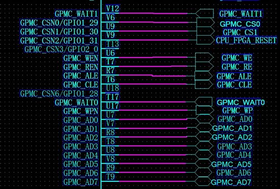
           According to the schematic above posts, I would like to achieve a gpmc nandflash chip communication and a gpmc with FPGA simulation nandflash communication with the following steps:

          Step 1: By the GPMC CS0 and nandflash (K9F1G08U0D) communications, this is easy to debug, have been through.

           Step 2: Through the GPMC CS1 and FPGA simulation nandflash read and write timing sequence for communication, this step has not been transferred through, please help heroes.

           I have been more puzzled, CS1 initialization and device files with FPGA simulation nandflash now CS0 and CS1 are shared with other signals, initialization should be initialized once is good.

Schematic follows:

Initialization code is as follows:

/* Pin mux for nand flash module */
static struct pinmux_config nand_pin_mux[] = {
{"gpmc_ad0.gpmc_ad0", OMAP_MUX_MODE0 | AM33XX_PIN_INPUT_PULLUP},
{"gpmc_ad1.gpmc_ad1", OMAP_MUX_MODE0 | AM33XX_PIN_INPUT_PULLUP},
{"gpmc_ad2.gpmc_ad2", OMAP_MUX_MODE0 | AM33XX_PIN_INPUT_PULLUP},
{"gpmc_ad3.gpmc_ad3", OMAP_MUX_MODE0 | AM33XX_PIN_INPUT_PULLUP},
{"gpmc_ad4.gpmc_ad4", OMAP_MUX_MODE0 | AM33XX_PIN_INPUT_PULLUP},
{"gpmc_ad5.gpmc_ad5", OMAP_MUX_MODE0 | AM33XX_PIN_INPUT_PULLUP},
{"gpmc_ad6.gpmc_ad6", OMAP_MUX_MODE0 | AM33XX_PIN_INPUT_PULLUP},
{"gpmc_ad7.gpmc_ad7", OMAP_MUX_MODE0 | AM33XX_PIN_INPUT_PULLUP},
{"gpmc_wait0.gpmc_wait0", OMAP_MUX_MODE0 | AM33XX_PIN_INPUT_PULLUP},
{"gpmc_wpn.gpmc_wpn", OMAP_MUX_MODE7 | AM33XX_PIN_INPUT_PULLUP},
{"gpmc_csn0.gpmc_csn0", OMAP_MUX_MODE0 | AM33XX_PULL_DISA},
{"gpmc_advn_ale.gpmc_advn_ale", OMAP_MUX_MODE0 | AM33XX_PULL_DISA},
{"gpmc_oen_ren.gpmc_oen_ren", OMAP_MUX_MODE0 | AM33XX_PULL_DISA},
{"gpmc_wen.gpmc_wen", OMAP_MUX_MODE0 | AM33XX_PULL_DISA},
{"gpmc_ben0_cle.gpmc_ben0_cle", OMAP_MUX_MODE0 | AM33XX_PULL_DISA},
{NULL, 0},

}

static void evm_nand_init(int evm_id, int profile)
{
struct omap_nand_platform_data *pdata;
struct omap_nand_platform_data *pdata1;
struct gpmc_devices_info gpmc_device[2] = {
{ NULL, 0 },
{ NULL, 0 },
};
pr_info("file:%s,func:%s,line:%d\n",__FILE__,__func__,__LINE__);
setup_pin_mux(nand_pin_mux);
pdata = omap_nand_init(am335x_nand_partitions,
ARRAY_SIZE(am335x_nand_partitions), 0, 0,
&am335x_nand_timings);
if (!pdata)
return;
pdata->ecc_opt =OMAP_ECC_BCH8_CODE_HW;
pdata->elm_used = true;
gpmc_device[0].pdata = pdata;
gpmc_device[0].flag = GPMC_DEVICE_NAND;
pr_info("file:%s,func:%s,line:%d cs:%d\n",__FILE__,__func__,__LINE__,pdata->cs);
pdata1 = omap_nand_init(am335x_nand_partitions,
ARRAY_SIZE(am335x_nand_partitions), 1, 0,
&am335x_nand_timings);
if (!pdata1)
return;
pdata1->ecc_opt =OMAP_ECC_BCH8_CODE_HW;
pdata1->elm_used = true;
gpmc_device[1].pdata = pdata1;
gpmc_device[1].flag = GPMC_DEVICE_NAND;
pr_info("file:%s,func:%s,line:%d cs:%d\n",__FILE__,__func__,__LINE__,pdata->cs);
omap_init_gpmc(gpmc_device, sizeof(gpmc_device));
omap_init_elm();

  • I can see no pinmux for GPMC_CS1. Are you sure your FPGA emulates NAND Flash exactly?

  • Thank you Biser Gatchev-XID ..

    Sorry, forgot to copy CS1, I now add up, I would like to ask how to use CS1 and FPGA simulation Nandflash communication

    Initialization code is as follows:

    /* Pin mux for nand flash module */
    static struct pinmux_config nand_pin_mux[] = {
    {"gpmc_ad0.gpmc_ad0", OMAP_MUX_MODE0 | AM33XX_PIN_INPUT_PULLUP},
    {"gpmc_ad1.gpmc_ad1", OMAP_MUX_MODE0 | AM33XX_PIN_INPUT_PULLUP},
    {"gpmc_ad2.gpmc_ad2", OMAP_MUX_MODE0 | AM33XX_PIN_INPUT_PULLUP},
    {"gpmc_ad3.gpmc_ad3", OMAP_MUX_MODE0 | AM33XX_PIN_INPUT_PULLUP},
    {"gpmc_ad4.gpmc_ad4", OMAP_MUX_MODE0 | AM33XX_PIN_INPUT_PULLUP},
    {"gpmc_ad5.gpmc_ad5", OMAP_MUX_MODE0 | AM33XX_PIN_INPUT_PULLUP},
    {"gpmc_ad6.gpmc_ad6", OMAP_MUX_MODE0 | AM33XX_PIN_INPUT_PULLUP},
    {"gpmc_ad7.gpmc_ad7", OMAP_MUX_MODE0 | AM33XX_PIN_INPUT_PULLUP},
    {"gpmc_wait0.gpmc_wait0", OMAP_MUX_MODE0 | AM33XX_PIN_INPUT_PULLUP},
    {"gpmc_wpn.gpmc_wpn", OMAP_MUX_MODE7 | AM33XX_PIN_INPUT_PULLUP},
    {"gpmc_csn0.gpmc_csn0", OMAP_MUX_MODE0 | AM33XX_PULL_DISA},

    {"gpmc_csn1.gpmc_csn1", OMAP_MUX_MODE0 | AM33XX_PULL_DISA},
    {"gpmc_advn_ale.gpmc_advn_ale", OMAP_MUX_MODE0 | AM33XX_PULL_DISA},
    {"gpmc_oen_ren.gpmc_oen_ren", OMAP_MUX_MODE0 | AM33XX_PULL_DISA},
    {"gpmc_wen.gpmc_wen", OMAP_MUX_MODE0 | AM33XX_PULL_DISA},
    {"gpmc_ben0_cle.gpmc_ben0_cle", OMAP_MUX_MODE0 | AM33XX_PULL_DISA},
    {NULL, 0},

    }

    static void evm_nand_init(int evm_id, int profile)
    {
    struct omap_nand_platform_data *pdata;
    struct omap_nand_platform_data *pdata1;
    struct gpmc_devices_info gpmc_device[2] = {
    { NULL, 0 },
    { NULL, 0 },
    };
    pr_info("file:%s,func:%s,line:%d\n",__FILE__,__func__,__LINE__); 
    setup_pin_mux(nand_pin_mux);
    pdata = omap_nand_init(am335x_nand_partitions,
    ARRAY_SIZE(am335x_nand_partitions), 0, 0,
    &am335x_nand_timings);
    if (!pdata)
    return;
    pdata->ecc_opt =OMAP_ECC_BCH8_CODE_HW;
    pdata->elm_used = true;
    gpmc_device[0].pdata = pdata;
    gpmc_device[0].flag = GPMC_DEVICE_NAND;
    pr_info("file:%s,func:%s,line:%d cs:%d\n",__FILE__,__func__,__LINE__,pdata->cs);
    pdata1 = omap_nand_init(am335x_nand_partitions,
    ARRAY_SIZE(am335x_nand_partitions), 1, 0,
    &am335x_nand_timings);
    if (!pdata1)
    return;
    pdata1->ecc_opt =OMAP_ECC_BCH8_CODE_HW;
    pdata1->elm_used = true;
    gpmc_device[1].pdata = pdata1;
    gpmc_device[1].flag = GPMC_DEVICE_NAND;
    pr_info("file:%s,func:%s,line:%d cs:%d\n",__FILE__,__func__,__LINE__,pdata->cs);
    omap_init_gpmc(gpmc_device, sizeof(gpmc_device));
    omap_init_elm();
    }

  • Hi,

    Can you help me explain how I now only need to achieve to read and write timing sequence through CS1, other nandflash the ECC, erase and so do not need to achieve, thank you very much