This Wiki entry:
processors.wiki.ti.com/.../Rebuilding_the_Flash_and_Boot_Utils_Package
on section:
ARM Compiler Tools (CodeSourcery G++ Lite)
instructs the user to download CodeSourcery G++ Lite. Unfortunately Mentor Graphics has ended CodeSourcery and no longer allows downloads of their Lite edition. The only option is to purchase the commercial CodeSourcery Code Bench
www.mentor.com/.../overview
Is there an alternate toolchain or can TI provide an alternate method to complete this build?
UPDATE:
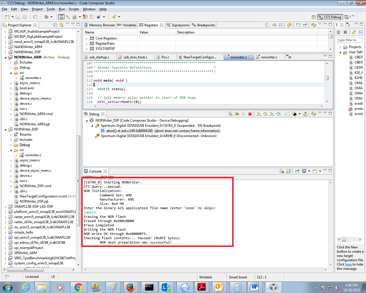
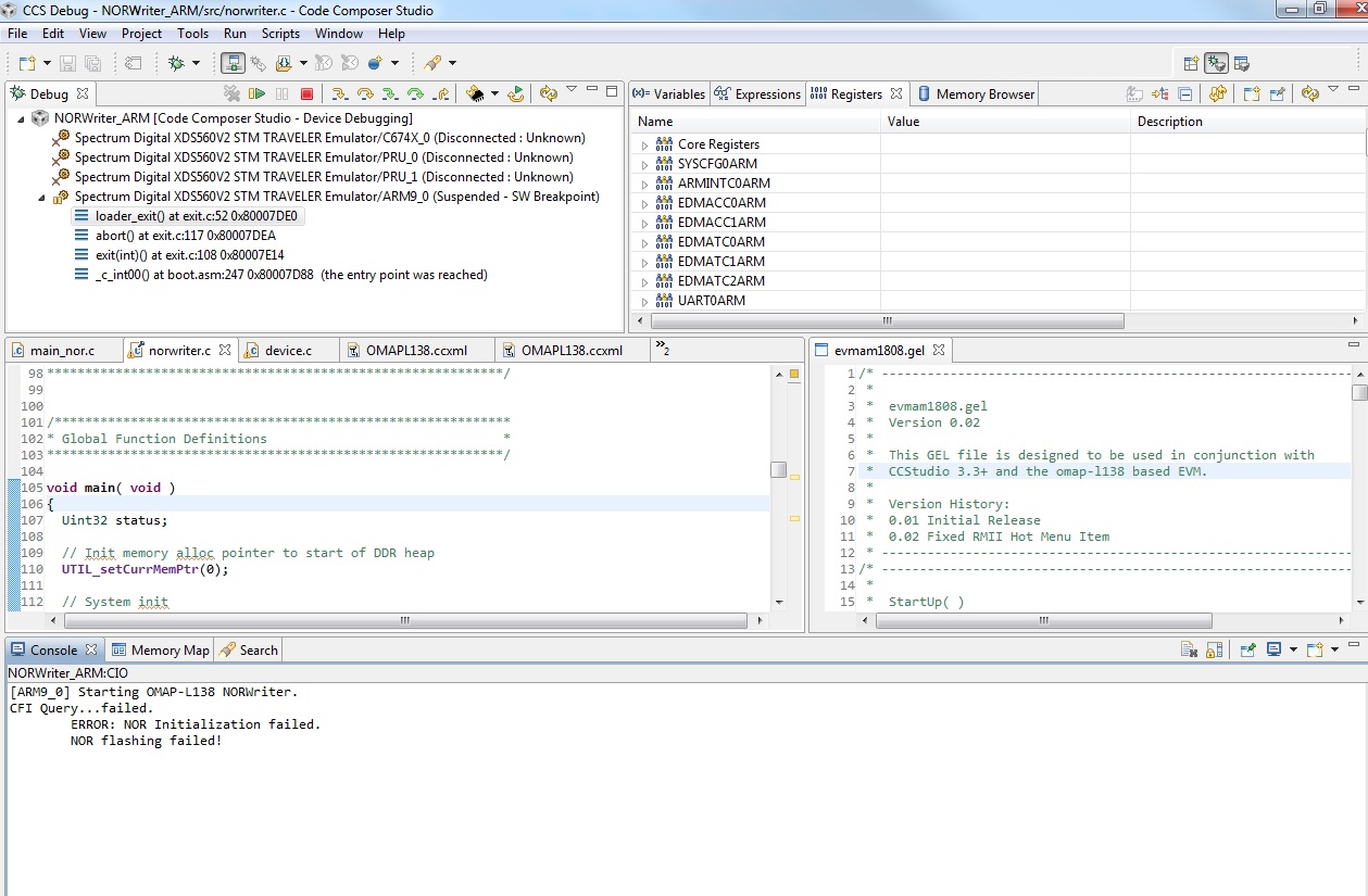
Inside OMAP-L138_FlashAndBootUtils_2_40 I found OMAP-L138_FlashAndBootUtils_2_40\OMAP-L138\CCS\NORWriter. This project builds in CCS 5.5, connects to my board, and begins to run on the ARM9. However, it hangs on line
// Initialize NOR Flash hNorInfo = NOR_open((Uint32)LOCAL_norBase, DEVICE_BUSWIDTH_16BIT );
inside of norwriter.c
After stepping through, it looks like line 142 of async_mem.c never returns:
(*hAsyncMemInfo->hDeviceInfo->fxnInit)(hAsyncMemInfo);
I have a TMDSSGI-EVML138 with an OMAP-L138/AM1808. I have successfully run a CCS hello world with UART, and verified I have a d800k008 via JTAG. Am I using an incorrect NOR flash writer?