This thread has been locked.

If you have a related question, please click the "Ask a related question" button in the top right corner. The newly created question will be automatically linked to this question.

Linux/dra726: Issue with UART2 with LIN device

Part Number: DRA726
Other Parts Discussed in Thread: DRA72, TPS51200, TLV320AIC3104

Tool/software: Linux

I have some issues with UART2 and can't seem to find a solution. Transmission works perfectly. I get the 1.3 msec break using a lower baud rate.

All scope signals look good, the timings are identical to the ones I have with our gauges with an old Jujitsu processor. I am able to get the slave gauges working as well as warning lights.

The problem arises with the input modules or whenever I send messages that require a response from the gauges or input modules.

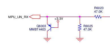
The signals are OK on the scope both at LIN_OUT and MPU_LIN_RX but I get no signal at the uart RX line.

If I change to use GPIO instead of UART pins I am able to toggle the TX and read the status on the RX Line.

I tried both blocking and non blocking modes, with select and without select.

I also tried a regular uart program and command line access with echo and cat, I cannot read anything from UART2

I have no issue with UART1 or UART3. I haven't tried UART9 yet.

I provided the schematic to Nicolas Le Lan (France). ACTIA's home base is ACTIA Automotive in France. ACTIA Corp is in Indiana but our TI contacts are those of ACTIA Automotive.

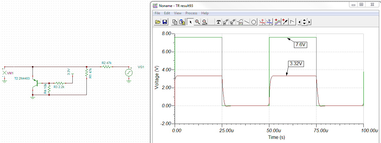
The circuits does the correct voltage conversion from 3.3V to 7.6V which is the voltage used by our gauges and warning modules.

Michel Catudal

ACTIA Corp

  • Hi Michel,

    I have forwarded your question to UART expert.

    Regards,
    Yordan
  • Hi Michel,
    Am I understanding correct? You can measure a data incoming on the processor RX pin, but UART2 is not firing any interrupt? How much data is expected in one data frame?

    regards,
    Stan
  • Hi Michel,
    In addition to the question asked by Stan above, please provide below.

    1. Please share a simple blaock diagram of teh connections if possible.<br>
    2. Have you checked UART2 pinmux conifguration in bootloader? Share the pinmux entries.
    3. Have you update dteh device tree node to reflect your ocnnections. Please share your board dts file.

    Also try to do a loopback test to see if the clocks and pinmuxing is done properly.

    You can do this in two ways
    1. Internal loopback - using a testutility like "serialcheck" processors.wiki.ti.com/.../Processor_SDK_Linux_Automotive_FAQ

    2. External loop back - connecting the pins together using a jumper. Do the sam etest mentione din above link without "-k" argument.

    Regards,
    RK
  • In my board mux_data.h  I tried a few different ones

      { UART2_RXD, (M0 | PIN_INPUT_PULLUP) },                    /* uart2_rxd.uart2_rxd */

      { UART2_TXD, (M0 | PIN_INPUT_PULLUP) },                    /* uart2_txd.uart2_txd */  

      { UART2_RXD, (M0 | PIN_INPUT) },                    /* uart2_rxd.uart2_rxd */

      { UART2_TXD, (M0 | PIN_INPUT) },                    /* uart2_txd.uart2_txd */  

      { UART2_RXD, (M0 | PIN_INPUT) },                                  /* uart2_rxd.uart2_rxd */

      { UART2_TXD, (M0 | PIN_OUTPUT) },                              /* uart2_txd.uart2_txd */  

      { UART2_RXD, (M0 | PIN_INPUT_PULLUP) },                    /* uart2_rxd.uart2_rxd */

      { UART2_TXD, (M0 | PIN_OUTPUT_PULLUP) },                    /* uart2_txd.uart2_txd */  

    It is a LIN circuitry so the TX is fed back to the RX. There is level translation since our supply on the gauge is 7.6V. The output is inverted twice, the input is not inverted, just kept from exceeding 3.3V

    The signal appears exactly as expected at the processor pin, from zero to 3.3V. The gauge always responds.

    I have tried several ways for the dts, at first I had the uart2 same as uart1. uart1 is used to program ans STM32 using ST bootloader. I then added some extra stuff like I had for uart3 which is used for the serial debug.

    That didn't change anything.

    The signal fed to that circuit is the LIN Signal which varies between 0 and 7.6V

    /*
     * Copyright (C) 2017 ACTIA Corp
     * Copyright (C) 2014 Texas Instruments Incorporated - http://www.ti.com/
     *
     * This program is free software; you can redistribute it and/or modify
     * it under the terms of the GNU General Public License version 2 as
     * published by the Free Software Foundation.
     */
    /dts-v1/;

    #include "dra72x.dtsi"
    #include <dt-bindings/gpio/gpio.h>
    #include <dt-bindings/net/ti-dp83867.h>

    / {
        compatible = "ti,dra722", "ti,dra72", "ti,dra7";

        model = "ACTIA Global Display";

        aliases {
            display0 = &lcd0;
            sound0 = &snd0;
        };

        memory {
            device_type = "memory";
            reg = <0x0 0x80000000
                   0x0 0x40000000>; /* 1GB */
        };

        reserved_mem: reserved-memory {
            #address-cells = <2>;
            #size-cells = <2>;
            ranges;

                    ipu2_cma_pool: ipu2_cma@95800000 {
                            compatible = "shared-dma-pool";
                            reg = <0x0 0x95800000 0x0 0x3800000>;
                            reusable;
                            status = "okay";
                    };

                ipu1_cma_pool: ipu1_cma@9d000000 {
                compatible = "shared-dma-pool";
                reg = <0x0 0x9d000000 0x0 0x2000000>;
                reusable;
                status = "okay";
            };
        };

            lcd0: display {
            compatible = "panel-dpi";

                    label = "lcd0";

            backlight = <&lcd_bl>;

                    panel-timing {
                            clock-frequency = <93688800>;
                            hactive = <1920>;
                            vactive = <720>;
                            hfront-porch = <115>;
                            hback-porch = <20>;
                            hsync-len = <5>;
                            vback-porch = <3>;
                            vfront-porch = <32>;
                            vsync-len = <3>;
                            hsync-active = <0>;
                            vsync-active = <0>;
                            de-active = <1>;
                            pixelclk-active = <1>;
                    };

                    port {
                            lcd_in: endpoint {
                                    remote-endpoint = <&dpi_out>;
                            };
                    };
            };

        lcd_bl: backlight {
                    compatible = "pwm-backlight";
                pinctrl-names = "default";
                    pinctrl-0 = <&bl_pwm_pins>;

                    pwms = <&ehrpwm0 0 50000 0>;

                    enable-gpios = <&gpio6 6 GPIO_ACTIVE_HIGH>;

                    /* 0 to 255 */
                    brightness-levels =
                <0  1  2  3  4  5  6  7  8  9 10 11 12 13 14 15 16 17 18 19
                            20 21 22 23 24 25 26 27 28 29 30 31 32 33 34 35 36 37 38 39
                40 41 42 43 44 45 46 47 48 49 50 51 52 53 54 55 56 57 58 59
                60 61 62 63 64 65 66 67 68 69 70 71 72 73 74 75 76 77 78 79
                80 81 82 83 84 85 86 87 88 89 90 91 92 93 94 95 96 97 98 99
                100 101 102 103 104 105 106 107 108 109 110 111 112 113 114 115 116 117 118 119
                120 121 122 123 124 125 126 127 128 129 130 131 132 133 134 135 136 137 138 139
                140 141 142 143 144 145 146 147 148 149 150 151 152 153 154 155 156 157 158 159
                160 161 162 163 164 165 166 167 168 169 170 171 172 173 174 175 176 177 178 179
                180 181 182 183 184 185 186 187 188 189 190 191 192 193 194 195 196 197 198 199
                200 201 202 203 204 205 206 207 208 209 210 211 212 213 214 215 216 217 218 219
                220 221 222 223 224 225 226 227 228 229 230 231 233 232 234 234 236 237 238 239
                240 241 242 243 244 245 246 247 248 249 250 251 252 253 254 255>;

                    default-brightness-level = <127>;
            };

        vdd_5v0: fixedregulator-vdd_5v0 {
                    /* Controlled by STMPU_PWR_CONTR_INV */
            compatible = "regulator-fixed";
            regulator-name = "vdd_5v0";
            regulator-min-microvolt = <5000000>;
            regulator-max-microvolt = <5000000>;
            regulator-always-on;
            regulator-boot-on;
        };

        vdd_3v3: fixedregulator-vdd_3v3 {
            compatible = "regulator-fixed";
            regulator-name = "vdd_3v3";
            regulator-min-microvolt = <3300000>;
            regulator-max-microvolt = <3300000>;
            regulator-always-on;
            regulator-boot-on;
        };

            vtt_fixed: fixedregulator-vtt {
                    /* TPS51200 */
                    compatible = "regulator-fixed";
                    regulator-name = "vtt_fixed";
                    vin-supply = <&smps5_reg>;
                    regulator-min-microvolt = <3300000>;
                    regulator-max-microvolt = <3300000>;
                    regulator-always-on;
                    regulator-boot-on;
                    enable-active-high;
                    gpio = <&gpio6 17 GPIO_ACTIVE_HIGH>;
            };

        snd0: sound@0 {
            compatible = "simple-audio-card";
            simple-audio-card,name = "Global Display";
            simple-audio-card,widgets =
                "Line", "Line Out",
                "Line", "Line In";
            simple-audio-card,routing =
                "Line Out",    "LLOUT",
                "Line Out",    "RLOUT",
                "MIC2L",    "Line In",
                "MIC2R",    "Line In";
            simple-audio-card,format = "dsp_b";
            simple-audio-card,bitclock-master = <&sound0_master>;
            simple-audio-card,frame-master = <&sound0_master>;
            simple-audio-card,bitclock-inversion;

            simple-audio-card,cpu {
                sound-dai = <&mcasp3>;
            };

            sound0_master: simple-audio-card,codec {
                sound-dai = <&tlv320aic3104>;
                clocks = <&clkout2_clk>;
            };
        };
    };

    &dra7_pmx_core {
        uart2_pins_default: uart2_pins_default {
            pinctrl-single,pins = <
                0x3f0 (PIN_INPUT_PULLUP | MUX_MODE0)  /* uart2_rxd.uart2_rxd  */
                0x3f4 (PIN_OUTPUT_PULLUP | MUX_MODE0) /* uart2_txd.uart2_txd  */
            >;
        };

        uart3_pins_default: uart3_pins_default {
            pinctrl-single,pins = <
                0x248 (PIN_INPUT_PULLUP | MUX_MODE0) /* uart3_rxd.gpio5_18 */
                0x24c (PIN_OUTPUT_PULLDOWN | MUX_MODE0) /* uart3_txd.gpio5_19 */
            >;
        };

        mmc1_pins_default: mmc1_pins_default {
            pinctrl-single,pins = <
                0x354 (PIN_INPUT_PULLUP | MUX_MODE0) /* mmc1_clk.clk */
                0x358 (PIN_INPUT_PULLUP | MUX_MODE0) /* mmc1_cmd.cmd */
                0x35c (PIN_INPUT_PULLUP | MUX_MODE0) /* mmc1_dat0.dat0 */
                0x360 (PIN_INPUT_PULLUP | MUX_MODE0) /* mmc1_dat1.dat1 */
                0x364 (PIN_INPUT_PULLUP | MUX_MODE0) /* mmc1_dat2.dat2 */
                0x368 (PIN_INPUT_PULLUP | MUX_MODE0) /* mmc1_dat3.dat3 */
            >;
        };

        mmc1_pins_hs: pinmux_mmc1_hs_pins {
            pinctrl-single,pins = <
                0x354 (PIN_INPUT_PULLUP | MUX_MODE0) /* mmc1_clk.clk */
                0x358 (PIN_INPUT_PULLUP | MUX_MODE0) /* mmc1_cmd.cmd */
                0x35c (PIN_INPUT_PULLUP | MUX_MODE0) /* mmc1_dat0.dat0 */
                0x360 (PIN_INPUT_PULLUP | MUX_MODE0) /* mmc1_dat1.dat1 */
                0x364 (PIN_INPUT_PULLUP | MUX_MODE0) /* mmc1_dat2.dat2 */
                0x368 (PIN_INPUT_PULLUP | MUX_MODE0) /* mmc1_dat3.dat3 */
            >;
        };

            mmc2_pins_default: mmc2_pins_default {
                    pinctrl-single,pins = <
                            0x9c (PIN_INPUT_PULLUP | MUX_MODE1) /* gpmc_a23.mmc2_clk */
                            0xb0 (PIN_INPUT_PULLUP | MUX_MODE1) /* gpmc_cs1.mmc2_cmd */
                            0xa0 (PIN_INPUT_PULLUP | MUX_MODE1) /* gpmc_a24.mmc2_dat0 */
                            0xa4 (PIN_INPUT_PULLUP | MUX_MODE1) /* gpmc_a25.mmc2_dat1 */
                            0xa8 (PIN_INPUT_PULLUP | MUX_MODE1) /* gpmc_a26.mmc2_dat2 */
                            0xac (PIN_INPUT_PULLUP | MUX_MODE1) /* gpmc_a27.mmc2_dat3 */
                            0x8c (PIN_INPUT_PULLUP | MUX_MODE1) /* gpmc_a19.mmc2_dat4 */
                            0x90 (PIN_INPUT_PULLUP | MUX_MODE1) /* gpmc_a20.mmc2_dat5 */
                            0x94 (PIN_INPUT_PULLUP | MUX_MODE1) /* gpmc_a21.mmc2_dat6 */
                            0x98 (PIN_INPUT_PULLUP | MUX_MODE1) /* gpmc_a22.mmc2_dat7 */
                    >;
            };

        mmc2_pins_hs: pinmux_mmc2_hs_pins {
            pinctrl-single,pins = <
                0x9c (PIN_INPUT_PULLUP | MUX_MODE1) /* gpmc_a23.mmc2_clk */
                0xb0 (PIN_INPUT_PULLUP | MUX_MODE1) /* gpmc_cs1.mmc2_cmd */
                0xa0 (PIN_INPUT_PULLUP | MUX_MODE1) /* gpmc_a24.mmc2_dat0 */
                0xa4 (PIN_INPUT_PULLUP | MUX_MODE1) /* gpmc_a25.mmc2_dat1 */
                0xa8 (PIN_INPUT_PULLUP | MUX_MODE1) /* gpmc_a26.mmc2_dat2 */
                0xac (PIN_INPUT_PULLUP | MUX_MODE1) /* gpmc_a27.mmc2_dat3 */
                0x8c (PIN_INPUT_PULLUP | MUX_MODE1) /* gpmc_a19.mmc2_dat4 */
                0x90 (PIN_INPUT_PULLUP | MUX_MODE1) /* gpmc_a20.mmc2_dat5 */
                0x94 (PIN_INPUT_PULLUP | MUX_MODE1) /* gpmc_a21.mmc2_dat6 */
                0x98 (PIN_INPUT_PULLUP | MUX_MODE1) /* gpmc_a22.mmc2_dat7 */
            >;
        };
        wlan_pins: pinmux_wlan_pins {
            pinctrl-single,pins = <
                0x37c (PIN_INPUT_PULLUP | MUX_MODE0)    /* mmc3_clk.mmc3_clk */
                0x380 (PIN_INPUT_PULLUP | MUX_MODE0)    /* mmc3_cmd.mmc3_cmd */
                0x384 (PIN_INPUT_PULLUP | MUX_MODE0)    /* mmc3_dat0.mmc3_dat0 */
                0x388 (PIN_INPUT_PULLUP | MUX_MODE0)    /* mmc3_dat1.mmc3_dat1 */
                0x38c (PIN_INPUT_PULLUP | MUX_MODE0)    /* mmc3_dat2.mmc3_dat2 */
                    0x390 (PIN_INPUT_PULLUP | MUX_MODE3)    /* mmc3_dat3.mmc3_dat3 */
                0x3ec (PIN_OUTPUT | MUX_MODE14)        /* uart1_rtsn.gpio7_25 - WLAN_EN */
            >;
        };

            mcspi4_pins: pinmux_mcspi4_pins {
                    pinctrl-single,pins = <
                            0x060 (PIN_OUTPUT | MUX_MODE8)          /* gpmc_a8.spi4_sclk */
                            0x064 (PIN_INPUT | MUX_MODE8)           /* gpmc_a9.spi4_d1 */
                            0x068 (PIN_OUTPUT | MUX_MODE8)          /* gpmc_a10.spi4_d0 */
                            0x06c (PIN_OUTPUT | MUX_MODE8)          /* gpmc_a11.spi4_cs0 */
                    >;
            };

        bl_pwm_pins: pinmux_bl_pwm_pins {
            pinctrl-single,pins = <
                0x164 (PIN_OUTPUT | MUX_MODE10)  /* vin2a_vsync0.ehrpwm1A */
            >;
        };
    };

    /* I2C */

    &i2c1 {
        status = "okay";
        clock-frequency = <400000>;

        tps65917: tps65917@58 {
            compatible = "ti,tps65917";
            reg = <0x58>;

            interrupts = <GIC_SPI 2 IRQ_TYPE_NONE>;  /* IRQ_SYS_1N */
            interrupt-controller;
            #interrupt-cells = <2>;

            ti,system-power-controller;

            tps65917_pmic {
                compatible = "ti,tps65917-pmic";

                smps1-in-supply = <&vdd_3v3>;
                smps2-in-supply = <&vdd_3v3>;
                smps3-in-supply = <&vdd_3v3>;
                smps4-in-supply = <&vdd_3v3>;
                smps5-in-supply = <&vdd_3v3>;
                ldo1-in-supply = <&vdd_3v3>;
                ldo2-in-supply = <&vdd_3v3>;
                ldo3-in-supply = <&vdd_3v3>;
                ldo4-in-supply = <&vdd_5v0>;
                ldo5-in-supply = <&vdd_3v3>;

                tps65917_regulators: regulators {
                    smps1_reg: smps1 {
                        /* VDD_MPU */
                        regulator-name = "smps1";
                        regulator-min-microvolt = <850000>;
                        regulator-max-microvolt = <1250000>;
                        regulator-always-on;
                        regulator-boot-on;
                    };

                    smps2_reg: smps2 {
                        /* VDD_CORE */
                        regulator-name = "smps2";
                        regulator-min-microvolt = <850000>;
                        regulator-max-microvolt = <1150000>;
                        regulator-boot-on;
                        regulator-always-on;
                    };

                    smps3_reg: smps3 {
                        /* VDD_GPU IVA DSPEVE */
                        regulator-name = "smps3";
                        regulator-min-microvolt = <850000>;
                        regulator-max-microvolt = <1250000>;
                        regulator-boot-on;
                        regulator-always-on;
                    };

                    smps4_reg: smps4 {
                        /* VDDS1V8 */
                        regulator-name = "smps4";
                        regulator-min-microvolt = <1800000>;
                        regulator-max-microvolt = <1800000>;
                        regulator-always-on;
                        regulator-boot-on;
                    };

                    smps5_reg: smps5 {
                        /* VDD_DDR */
                        regulator-name = "smps5";
                        regulator-min-microvolt = <1350000>;
                        regulator-max-microvolt = <1350000>;
                        regulator-boot-on;
                        regulator-always-on;
                    };

                    ldo1_reg: ldo1 {
                        /* MMC1_3V3  */
                        regulator-name = "ldo1";
                        regulator-min-microvolt = <3300000>;
                        regulator-max-microvolt = <3300000>;
                        regulator-always-on;
                        regulator-boot-on;
                        regulator-allow-bypass;
                    };

                    ldo3_reg: ldo3 {
                        /* VDDA_1V8_PHY */
                        regulator-name = "ldo3";
                        regulator-min-microvolt = <1800000>;
                        regulator-max-microvolt = <1800000>;
                        regulator-boot-on;
                        regulator-always-on;
                    };

                    ldo4_reg: ldo4 {
                        /* VUSB_3V3 */
                        regulator-name = "ldo4";
                        regulator-min-microvolt = <3300000>;
                        regulator-max-microvolt = <3300000>;
                        regulator-boot-on;
                        regulator-always-on; /* avoid turning of debug serial port */
                    };

                    ldo5_reg: ldo5 {
                        /* VDDA_1V8_PLL */
                        regulator-name = "ldo5";
                        regulator-min-microvolt = <1800000>;
                        regulator-max-microvolt = <1800000>;
                        regulator-always-on;
                        regulator-boot-on;

                    };
                };
            };
        };
    };

    &i2c3 {
               status = "okay";
            clock-frequency = <200000>;

        tlv320aic3104: tlv320aic3104@18 {
            #sound-dai-cells = <0>;
            compatible = "ti,tlv320aic3104";
            reg = <0x18>;

            assigned-clocks = <&clkoutmux2_clk_mux>;
            assigned-clock-parents = <&sys_clk2_dclk_div>;

            gpio-reset = <&gpio3 29 GPIO_ACTIVE_LOW>;
            adc-settle-ms = <40>;
              AVDD-supply = <&vdd_3v3>;
            IOVDD-supply = <&vdd_3v3>;
            DRVDD-supply = <&vdd_3v3>;
            DVDD-supply = <&vdd_3v3>;

            status = "okay";
        };

    };

    &i2c4 {
            status = "okay";
            clock-frequency = <400000>;

            egalax_i2c@2a {

                    compatible = "eeti,egalax_i2c";

                    reg = <0x2a>;

                    interrupt-parent = <&gpio4>;
                    interrupts = <4 0>;
                    int-gpios = <&gpio4 17 0>;
                    reset-gpio = <&gpio4 18 GPIO_ACTIVE_HIGH>;

                    touchscreen-size-x = <1920>;
                    touchscreen-size-y = <720>;
            };
    };

    &i2c5 {
             status = "okay";
             reg = <0x18>;
             clock-frequency = <400000>;

             accel: lis2dh12@18 {
                  compatible = "st,lis2dh12";
             reg = <0x18>;
             };
    };

    /* UARTs */

    &uart1 {
        status = "okay";
    };

    &uart2 {
        status = "okay";
        interrupts-extended = <&crossbar_mpu GIC_SPI 68 IRQ_TYPE_LEVEL_HIGH>,
                      <&dra7_pmx_core 0x3f0>;
    };

    &uart3 {
        status = "okay";
        interrupts-extended = <&crossbar_mpu GIC_SPI 69 IRQ_TYPE_LEVEL_HIGH>,
                      <&dra7_pmx_core 0x248>;
    };

    &uart5 {
        status = "okay";
    };

    &uart9 { /* for bluetooth */
            status = "okay";
    };

    /* SPI Busses
       mcspi1 is used by TI-RTOS */

    &mcspi4 {
            status = "okay";
            pinctrl-names = "default";
            pinctrl-0 = <&mcspi4_pins>;
    };

    /* USB */

    &usb2_phy1 {
        phy-supply = <&ldo4_reg>;
            status = "okay";
    };

    &usb2_phy2 {
        phy-supply = <&ldo4_reg>;
            status = "okay";
    };

    &usb1 {
        dr_mode = "host";
            status = "okay";
    };

    &usb2 {
        dr_mode = "host";
            status = "okay";
    };

    &mmc1 {
            status = "okay";
        pinctrl-names = "default", "hs";
            pinctrl-0 = <&mmc1_pins_default>;
        pinctrl-1 = <&mmc1_pins_hs>;
            vmmc-supply = <&ldo1_reg>;
            bus-width = <4>;
            max-frequency = <192000000>;
            no-1-8-v;
    };

    &mmc2 {
            status = "okay";
        pinctrl-names = "default", "hs";
            pinctrl-0 = <&mmc2_pins_default>;
        pinctrl-1 = <&mmc2_pins_hs>;
            vmmc-supply = <&ldo1_reg>;
            bus-width = <8>;
            ti,non-removable;
            max-frequency = <192000000>;
            no-1-8-v;
    };

    &mac {
        slaves = <1>;
         status = "okay";
     };

    &cpsw_emac0 {
        phy-handle = <&dp83867_0>;
        phy-mode = "rgmii-id";
    };

    &davinci_mdio {
        dp83867_0: ethernet-phy@0 {
                    reg = <0>;
                    ti,rx-internal-delay = <DP83867_RGMIIDCTL_2_25_NS>;
                    ti,tx-internal-delay = <DP83867_RGMIIDCTL_250_PS>;
                    ti,fifo-depth = <DP83867_PHYCR_FIFO_DEPTH_8_B_NIB>;
                    ti,impedance-control = <0x1f>;
        };
    };

    &dss {
            status = "okay";
            ports {
                    #address-cells = <1>;
                    #size-cells = <0>;

                    port {
                            reg = <0>;

                            dpi_out: endpoint {
                                    remote-endpoint = <&lcd_in>;
                                    data-lines = <24>;
                            };
                    };
            };
    };

    &epwmss0 {
            status = "okay";
    };

    &ehrpwm0 {
            status = "okay";
    };

    &bb2d {
        status = "okay";
    };

    &mailbox5 {
        status = "okay";
        mbox_ipu1_ipc3x: mbox_ipu1_ipc3x {
        status = "okay";
        };
    };

    &mailbox6 {
           status = "okay";
           mbox_ipu2_ipc3x: mbox_ipu2_ipc3x {
           status = "okay";
           };
    };

    &mmu_ipu1 {
        status = "okay";
    };

    &mmu_ipu2 {
           status = "okay";
    };

    &ipu2 {
           status = "okay";
           memory-region = <&ipu2_cma_pool>;
           mboxes = <&mailbox6 &mbox_ipu2_ipc3x>;
           timers = <&timer3>;
           watchdog-timers = <&timer4>, <&timer9>;
    };

    &ipu1 {
        status = "okay";
        memory-region = <&ipu1_cma_pool>;
        mboxes = <&mailbox5 &mbox_ipu1_ipc3x>;
        timers = <&timer11>;
        watchdog-timers = <&timer7>, <&timer8>;
    };

    &oppdm_mpu {
        vdd-supply = <&smps1_reg>;
    };

    &oppdm_core {
        vdd-supply = <&smps2_reg>;
    };

    &oppdm_gpu {
        vdd-supply = <&smps3_reg>;
    };

    &oppdm_ivahd {
        vdd-supply = <&smps3_reg>;
    };

    &dss {
        status = "okay";
        vdda_video-supply = <&ldo5_reg>;
    };

  • I put two replies and none appear

    Michel
  • Michel,
    Just close the browser, clear cookies and try again. If you are trying to paste and image directly then it doesnt work - upload as an attachment.
    Regards,
    RK
  • Since the lines are connected together I used the duplex mode for 1 test

    root@actia-global-display:~# ./serialcheck -d /dev/ttyS1 -b 9600 -k -m d -f ./jj.dtb -l 2
    Needed 56 reads 1 writes loops 2 / 2
    cts: 0 dsr: 0 rng: 0 dcd: 0 rx: 186412 tx: 186412 frame 0 ovr 0 par: 0 brk: 0 buf_ovrr: 0

    With a similar test as on the info website

    First ssh Terminal

    root@actia-global-display:~# ./serialcheck -d /dev/ttyS1 -b 9600 -k -m r -f ./jj.dtb -l 2
    Needed 971 reads 0 writes loops 2 / 2
    cts: 0 dsr: 0 rng: 0 dcd: 0 rx: 186412 tx: 186412 frame 0 ovr 0 par: 0 brk: 0 buf_ovrr: 0


    Second ssh Terminal

    root@actia-global-display:~# ./serialcheck -d /dev/ttyS1 -b 9600 -k -m t -f ./jj.dtb -l 2
    Needed 0 reads 1 writes loops 2 / 2
    cts: 0 dsr: 0 rng: 0 dcd: 0 rx: 183216 tx: 183296 frame 0 ovr 0 par: 0 brk: 0 buf_ovrr: 0


    Michel
  • Michel,
    If the lines are ocnnected together then you can try without "-k" option to confirm if pad configuration is correct.

    Regards,
    RK
  • root@actia-global-display:~# ./serialcheck -d /dev/ttyS1 -b 9600 -m d -f ./jj.dtb -l 2

    timeout, RX/TX: 0/93206
    Needed 0 reads 1 writes Oh oh, inconsistency at pos 0 (0x0).

    Original sample:
    00000000: d0 0d fe ed 00 01 6c 16 00 00 00 38 00 01 5e 58 ......l....8..^X
    00000010: 00 00 00 28 00 00 00 11 00 00 00 10 00 00 00 00 ...(............
    00000020: 00 00 0d be 00 01 5e 20 00 00 00 00 00 00 00 00 ......^ ........

    Received sample:
    00000000: 00 00 00 00 00 00 00 00 00 00 00 00 00 00 00 00 ................
    00000010: 00 00 00 00 00 00 00 00 00 00 00 00 00 00 00 00 ................
    00000020: 00 00 00 00 00 00 00 00 00 00 00 00 00 00 00 00 ................
    loops 1 / 2

    cts: 0 dsr: 0 rng: 0 dcd: 0 rx: 0 tx: 93206 frame 0 ovr 0 par: 0 brk: 0 buf_ovrr: 0

    root@actia-global-display:~# ./serialcheck -d /dev/ttyS1 -b 9600 -m r -f ./jj.dtb -l 2

    timeout, RX/TX: 0/0
    Needed 0 reads 0 writes Oh oh, inconsistency at pos 0 (0x0).

    Original sample:
    00000000: d0 0d fe ed 00 01 6c 16 00 00 00 38 00 01 5e 58 ......l....8..^X
    00000010: 00 00 00 28 00 00 00 11 00 00 00 10 00 00 00 00 ...(............
    00000020: 00 00 0d be 00 01 5e 20 00 00 00 00 00 00 00 00 ......^ ........

    Received sample:
    00000000: 00 00 00 00 00 00 00 00 00 00 00 00 00 00 00 00 ................
    00000010: 00 00 00 00 00 00 00 00 00 00 00 00 00 00 00 00 ................
    00000020: 00 00 00 00 00 00 00 00 00 00 00 00 00 00 00 00 ................
    loops 1 / 2

    cts: 0 dsr: 0 rng: 0 dcd: 0 rx: 0 tx: 4159 frame 0 ovr 0 par: 0 brk: 0 buf_ovrr: 0

    root@actia-global-display:~# ./serialcheck -d /dev/ttyS1 -b 9600 -m t -f ./jj.dtb -l 2
    Needed 0 reads 1 writes loops 2 / 2
    cts: 0 dsr: 0 rng: 0 dcd: 0 rx: 0 tx: 184313 frame 0 ovr 0 par: 0 brk: 0 buf_ovrr: 0
  • That is the input, the signal fed can vary between 0 and 7.6V

    Michel

  • Hi Michel,

    What is the logic 1 voltage measured on MPU_LIN_RX?  I don't think the PNP does it's mission to regulate at 3.3V. Bipolar transistors need -0.6V VEB to start conducting current. I.e. the transistor on the diagram does nothing up to 3.9V. Although 7.6V / 2 = 3.8V, because of the divider network, it is still bad for the processor pins.

  • Michel,

    We did a little simulation here. As you see the pnp is regulating at 3.3V only after we've added R3/R4 divider for a 2.75V base voltage.

    Without that network, all 3.8 volts were output.

    This might not solve your problem, but it is a major error of the design.

    Regards,

    Stan

  • Stan,

    Thank you, I will be passing this along with to our electronic design team.

    Michel