This thread has been locked.

If you have a related question, please click the "Ask a related question" button in the top right corner. The newly created question will be automatically linked to this question.

AM5728: PCIe external clock SI issues

Part Number: AM5728

Dear community,

we are using PCIe on our custom Board to communicate with a standard Intel Wifi-card and our custom FPGA. The clock is generated by a 9FGL0441 PCIe clock generator device.

Part of our hardware-test was the evaluation of the signal integrity of the PCIe clocks to:

  • WIFI-card
  • FPGA
  • AM5728

Measurements have been executed with a LeCroy SDA760Zi-A 6Ghz scope, using active differential probes with 6GHz bandwidth.

  • The clocks to WIFI and FPGA showed no/small signal integrity issues.
  • But the clock to the AM5728 CPU showed massive problems. Nevertheless, communication with WIFI-card and FPGA is working!

We did the same measurement on the AM5728-IDK and saw a similar effect. 

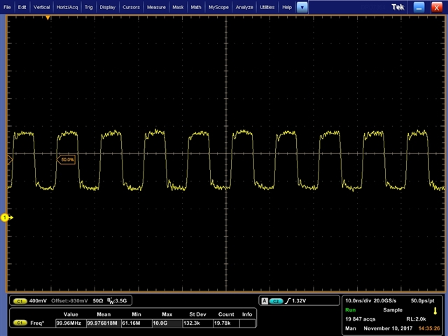
The attached pictures show the clock measurement right after startup and after some uptime. No difference if the device stays in u-boot or has a fully booted Linux.

Has anybody else observed this? Currently we don't experience problems but we want to make sure this does not become a problem when we put this into a product.

Regards,

Michael

  • Michael,

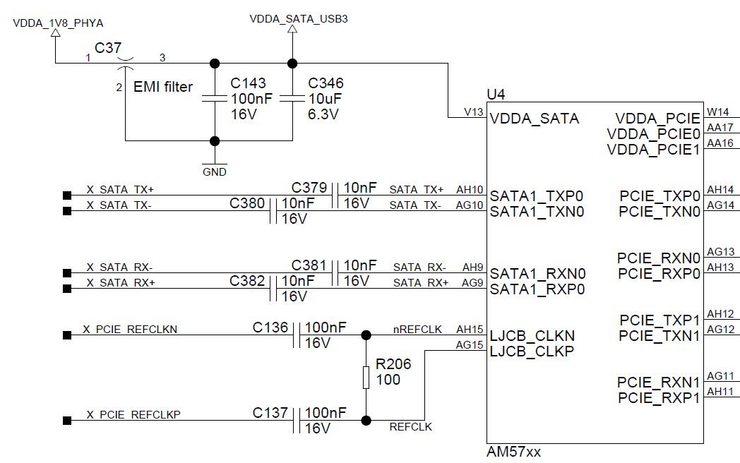
    Does your board contain input circuitry consistent with the guidance in the latest version of the AM5728 DM (SPRS953C) in section 8.7 LJCB_REFN/P Connections?

    Tom

  • Hi Michael,

    I took a look at this in our lab today and wasn't able to repro the issue on either AM571x IDK or AM572x IDK. I'm using the current Linux SDK (4.01).

    I let the boards sit at the Linux prompt for an hour and never saw the waveform change. I've attached the AM572x IDK waveform here.

  • Hi -DK-,

    is your measurement against ground or the differential signal over R581?

    This is our measurement on the IDK: 

    PCIe clock over R581 on IDK just after power up:

    The same after a few (20) seconds:

    Our fix (for our hardware) was to change from AC coupling to DC coupling – e.g. replace the coupling Cs with 0R.

    Then we got this signal (measured at input of AM5728) which looks much better:

    Regards,

    Michael

  • Hi Michael,
    I used a differential probe (Tek P6247) for my measurements. I just re-took them with no change in result.

    These signals should be AC coupled so we need to dig a bit deeper. My gut feeling is a mis-configured SERDES on the SoC side or clock contention from an inserted device. I could also lean toward a bad clock generator (or poor assembly of same) if you hadn't duplicated this on two different boards (yours + ours).

    Do you have something inserted in the IDK PCIe socket? My measurements are with nothing in the socket.
  • We are sorry explaining wrongly were we measured:

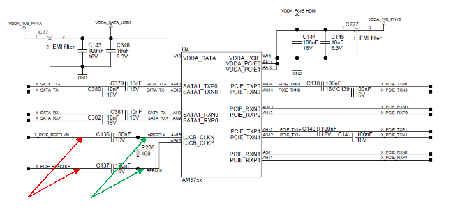
    If you measure at the position of the green arrows, the DC voltages are discharged immediately and you will observe a correct waveform of the clock.

    (Even with a differential probe !)


    If you measure at the position of the red arrows you will observe the distorted waveform as attached in the previous mails and the TI case.

    Immediately after power up, the shape of the clock signal is still correct, but after a short time you can observe that it is changing smoothly

    into its distorted shape.

    If then another probe is connected, even at only one green position, the clock turns back to its normal shape.


    Similar measurements on the TI IDK show exactly the same behavior.


    Martin

  • Sorry for the delay. I have been able to repro what you are seeing now, but I can't explain it offhand so I'm looping in others internally.

    I'll post updates here.
  • Martin,
    The consensus here is that this is a scope-induced artifact. The delayed distortion is caused by the caps discharging very slowly thru the scope itself.
  • Martin,

    Please post both single ended and differential scope captures for both the green and read points.  The expectation is that there is no DC bias imposed on the source side and that this shifts when the oscilloscope is added.  This DC-shift itself may be the cause of the observed distortion.

    Tom

  • Martin,

    What is the driving source for this clock?

    Tom

  • Dear Tom,

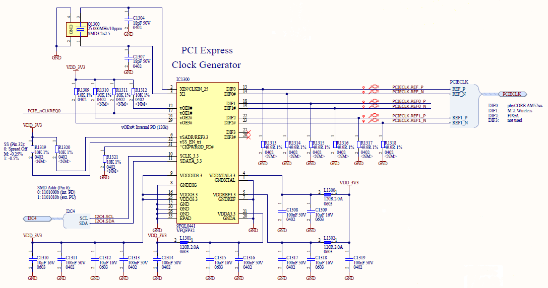
    we use the 9FGL0441 Clock-generator

    We are using PCIECLK_REFP/N for the Sitara. We could configure the clock-generator via I2C4 but our SW does not use of it.

    Martin 

  • Dear Tom,

    unfortunately we did not save the screens with the single ended measurements.


    Our clock driver (9FGL0441) has LP-HCSL outputs.

    Some Appnotes:

    https://www.idt.com/document/apn/879-low-power-hcsl-vs-traditional-hcsl

    https://www.idt.com/document/apn/891-driving-lvpecl-lvds-cml-and-sstl-logic-idts-universal-low-power-hcsl-outputs

    Your manuals do not include the internal details of the PCIe clock input circuitry,

    so we expect the following:

    The Sitara has no internal pullups/pulldowns for a DC reference on the PCIe clock input. This input will have an input bias current, which may be small but is not equal to zero. As the outer circuitry (even on the Sitara IDK) as well has no DC reference,

    This small current charges the coupling C's with the consequence of a distorted clock signal (if the input clamping diodes react).

    What happens, if we add a probe (at the green points) to the clock-lane - we add something like a DC reference, the C's discharge immediately via the inner impedance of the probe and the clock signal turns back into its correct shape.

    The same situation could be observed, as we changed to DC coupling - no distorted clock signal at all.


    Your manuals include no biunique definition, whether AC coupling must be used or DC coupling could be used.

    Can You please give us the advice, which is the correct way - DC coupling or DC reference at the Sitaras clk inputs and how.


    Kind regards

    Martin

  • Martin,

    The Data Manual provides recommended circuits for 2 types of clock drivers: HCSL and LVDS.  HCSL is a current mode driver and LVDS is a voltage mode driver.  Your driver uses a proprietary LP-HCSL which is not a current mode driver.  I recommend that you follow the guidance for the LVDS input which only has the DC-blocking caps and the differential 100-ohm termination.  This matches with your implementation.

    The LJCB input will generate its own DC bias.  This is compatible to HCSL but not with LVDS - that is why the DC-blocking caps are needed for LVDS.  You should not alter this DC-bias as seen at the green sample points.

    My request still stands - we need to see both single-ended and differential captures at both the read and green sample points.  Also, you indicate that the distortion is at the red sample points which are essentially at the clock driver output.  This needs to be discussed with that manufacturer.  You might need to add a DC path to ground for the LP-HCSL output signal.

    Tom

  • Dear  Tom,

    thanks for your answer - it took a while for creating the screen-shots you requested.

    Here again the schematics. We measured at X_PCIE_REFCLKP and REFCLK

    X_PCIE_REFCLKP directly after powerup:

    X_PCIE_REFCLKP 30s after powerup:

    REFCLK DC after connecting a 1 MOhm probe:

    and finally the REFCLK signal after connecting the probe:

    Please note the offset voltage InputAOffset

    Martin

  • Martin,

    These captures confirm that the issue is a DC-bias / DC ground reference problem on the driver side of the caps.  This needs to be resolved with the manufacturer of the clock driver.  I expect that some type of ground reference is needed due to a DC imbalance that saturates the driver.

    Tom