This thread has been locked.

If you have a related question, please click the "Ask a related question" button in the top right corner. The newly created question will be automatically linked to this question.

CCS/CCSTUDIO: C5517 LDOO voltage fault

Part Number: CCSTUDIO

Tool/software: Code Composer Studio

Hello everybody,

we developed a board TMS320C5517 provided with 1,3V core and 3.3V I/O.

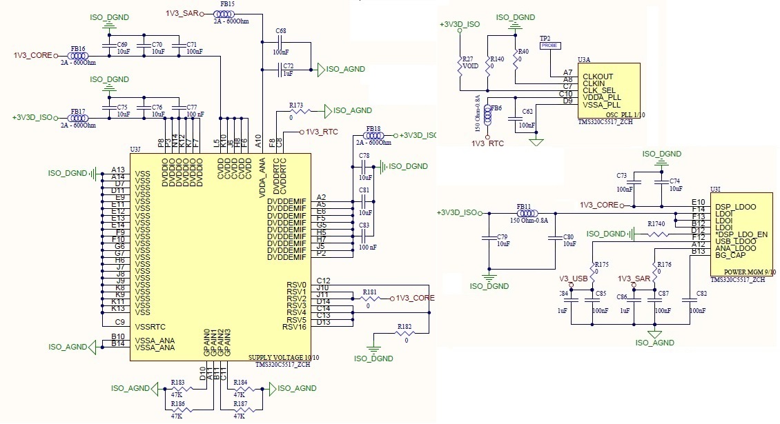
DSP power related schematics are attached.

We have a problem related to DSP LDO outputs (1V3_USB,1V3_SAR,1V3_CORE),

which on certain circustances simultaneously drop from the nominal level of 1,3V to about 1,0 V or less,

which is largely under specifications, and we believe could spoil the DSP.

First of all, in general what this voltage drop could mean ? 
Which feature of the board could effect this internally generated voltages ? 

Now here we explain the circumstances.

DSP is asynchronous EMIF interfaced to a FPGA, which in turn is the master for some slave ADCs.

When the FPGA is driving the ADCs control signal (MCLK,LRCLK,SCLK), as soon the ADCs are removed from Reset

all the DSP LCD outputs drop to 1,0 V or less: LDO outputs return to regular 1,3V as soon the ADCs are kept in Reset.

The problem is also not present if  we remove the ADCs from the board...

Please note that no direct digital HW interface exist between the ADCs and DSP; moreover in our tests,

we prevent DSP from driving the EMIF interface to FPGA. 

LDO dropout occour even if we stop the software (using a breakpoint) and we configure all the GPIO as inputs.

EBSR register is configured as follow:

GpioStatus = SYS_setEBSR(CSL_EBSR_FIELD_PPMODE,CSL_EBSR_PPMODE_1);
GpioStatus |= SYS_setEBSR(CSL_EBSR_FIELD_SP0MODE,CSL_EBSR_SP0MODE_3);
GpioStatus |= SYS_setEBSR(CSL_EBSR_FIELD_SP1MODE,CSL_EBSR_SP1MODE_2);
GpioStatus |= SYS_setEBSR(CSL_EBSR_FIELD_A15MODE,CSL_EBSR_A_MODE_0);
GpioStatus |= SYS_setEBSR(CSL_EBSR_FIELD_A16MODE,CSL_EBSR_A_MODE_0);
GpioStatus |= SYS_setEBSR(CSL_EBSR_FIELD_A17MODE,CSL_EBSR_A_MODE_0);
GpioStatus |= SYS_setEBSR(CSL_EBSR_FIELD_A18MODE,CSL_EBSR_A_MODE_0);
GpioStatus |= SYS_setEBSR(CSL_EBSR_FIELD_A19MODE,CSL_EBSR_A_MODE_0);
GpioStatus |= SYS_setEBSR(CSL_EBSR_FIELD_A20MODE,CSL_EBSR_A_MODE_0);

The 3V3D_ISO voltage providing the input at LDOI is stable to 3.3V, with a current draw of 140mA (3.3V regulator max current 500mA)

Measurig the current draw at the LDOs outputs we have:

DSP_LDOO: 24mA (max)

USB_LDOO: <1mA 

ANA_LDOO: <1mA

1V3_RTC voltage is stable, with no drop below 1.3V.

If we drive the RESET pin low while the ADCs are on and the LDO voltage is below 1V, DSP_LDOO, USB_LDOO, ANA_LDOO go back to 1.3V.

I also tried to exclude USB influence by removing R175, with no better results.

On these circumstances, what do you think could cause the LDOs outputs drop?

Could a GPIO conflict cause an LDO voltage drop?


Do not esitate to request us more informations.

Thank you for your attention.

  • We're looking into this.

    Best Regards,
    Yordan
  • Hi Stefano,

    This is a strange issue. All of the symptoms point to an over-current situation, but you say the voltages and currents are within the normal range. Have you checked the main power supply? Is it USB powered? Powered by a wall wort?

    How fast are you measuring the instantaneous current inrush when the ADCs start up? Maybe they need a bigger bulk capacitor.

    Does the C5517 ever go into RESET and reboot?
    When DSP_LDO is used the internal POR reset logic gets enabled, and monitors the DSP_LDO voltage. Reset is applied whenever DSP_LDO < 1V or so.

    What is SYSCLK frequency? For SYSCLK > 175MHz, 1.4V CVDD is required. The on-chip DSP_LDO is not capable of supplying 1.4V.

    What is DSP_LDO_V value in LDOCNTL?

    Try to isolate if one of the LDO outputs is the source of the voltage droop. Supply each LDO externally one by one. For example - supply 1.3V to CVDD and leave DSP_LDOO floating and repeat the experiment.

    If its not a power issue, then next guess is that noise is coupling in somewhere. Maybe noise on the supply or an coupling in from one of those ADC clocks. Perhaps you could try to change CLKIN to high and supply a 12MHz clock at CLKIN as an experiment.

    Do you have two TPS22929 gates for USB power sequencing - one from USB 1.3V to USB_3V3 and another (U62) from USB_3V3 to VBUS? What happens when the USB_LDO droops to 1V? Does it fall below the threshold, and then gate USB_3V3, which would stop the USB oscillator?

    I also wonder what would happen if you clocked the RTC oscillator, if that is possible. There are some power-related registers in the RTC domain...

    Please let us know what you find.

    Regards,
    Mark
  • Hi Mark,

    thank you for your support!

    After several tests I ended up "handling" the issue by: 

    1) Disabling the dsp LDO by setting DSP_LDO_EN pin to 3.3V.

    2) Provide 1V3_CORE, 1V3_USB voltagese with an external LDO (leaving DSP_LDOO,USB_LDOO floating).

    Everthing works ok now, USB communication included.

    Btw, still I'm not able to understand why if I use the internal DSP LDO the 1.3V voltage drops.

    Here my answers to your suggestions:

    This is a strange issue. All of the symptoms point to an over-current situation, but you say the voltages and currents are within the normal range. Have you checked the main power supply? Is it USB powered? Powered by a wall wort?

    It is not USB powered, no over current measured, main power supply stable to its normal operation.

    Does the C5517 ever go into RESET and reboot?

    No

    What is SYSCLK frequency? For SYSCLK > 175MHz, 1.4V CVDD is required. The on-chip DSP_LDO is not capable of supplying 1.4V.
    What is DSP_LDO_V value in LDOCNTL? 

    SYS CLK is 100MHz. I tried using a lower SYSCLK with no results. I also used an external CLK(88MHz), configured CLKSSEL=1,SYSCLKSEL=0,disabled all the DSP peripherals (PCGCR1 exept SYSCLK), and disabled PLL, still no results. I then used a test software with a simple main() function where I just turn off and on the adc, and the Vcore was still dropping with the ADC enable.

    Try to isolate if one of the LDO outputs is the source of the voltage droop. Supply each LDO externally one by one. For example - supply 1.3V to CVDD and leave DSP_LDOO floating and repeat the experiment.

    If I do so, I still see the dsp_ldoo dropping down.

    If its not a power issue, then next guess is that noise is coupling in somewhere. Maybe noise on the supply or an coupling in from one of those ADC clocks. Perhaps you could try to change CLKIN to high and supply a 12MHz clock at CLKIN as an experiment.

    With an oscilloscope I could see much noise, anyways even by providing an external CLK the proble sussist


    I also noticed that once the vcore drops, I'm not able to work with a sysclk higher than 100MHz.

    On the final stage of my test, nothing was mounted on my board exept the DSP and the ADC..

    What is the best solution if I provide the 1.3V with an external LDO? Should each 1.3V (CORE/USB/ANA) have their own LDO or it is enough to just use one external LDO? Is there an application note?

    Even if I was able to manage the problem with an external ldo, I would prefer to understand why the LDO is dropping, do you have any suggestions?

    Thank you for your time.

    Regards

    Stefano

  • Hi Stefano,

    Glad you found a work around, but I am also interested in the cause of the LDO dropping out. Can you probe the voltage of BG_CAP when the issue occurs? This is the reflects the reference voltage for the LDOs, and should be about 0.7V, I believe.

    What is the normal frequency of CLKIN  on your board?

    I'm not certain what is the maximum frequency that CLKIN can tolerate. The datasheet says it is 19.2MHz, but that is just to ensure that the bootloader does not configure the PLL too fast. There will also be a max frequency that the CLKIN input can tolerate. Id guess its around 50MHz, but not sure. Was it working well with 88MHz.

    See Table 5-7. PLL Clock Frequency Ranges in the datasheet.

    You can ensure that PLL settings are not out of range by using the attached PLL calculator to plug in your parameters and check that they are not out of range. This sheet also provides the bootloader PLL settings, so you can ensure that your CLKIN does not violate the PLL ranges when the bootloader is running.

    The fastest CLKIN without bootloader PLL setting violating PLL ranges: 26.041666MHz

    (Assumes the worst case of using the PLL to multiply the input clock by 3:

    From SPRABP1: While the bootloader tries to boot from SPI, McSPI, UHPI, USB, and UART, the clock generator is programmed to multiply the input clock by 3 and adjust the TIMER0 setting to 200 ms)

    If you suspect there is noise on CLKIN, perhaps you can use CLKOUT to verify that the SYSCLK is what you think it is (and is not seeing glitches that might cause overclocking).

    /cfs-file/__key/communityserver-discussions-components-files/791/0284.Phoenix_5F00_PLL_5F00_Calculator_5F00_with_5F00_Bootloader_5F00_config.xlsx

    Regards,
    Mark

  • Hi Mark,

    thanks again for your support!

    I used an external CLK just as a test for my issue: normally my board uses the 12MHz USB PLL, with a 100MHz SYSCLK derived as follow.

    I used CSL example as a referenze:

    PLL_Config pllCfg_100MHz = {0x2056, 0x0001, 0x0000,  0x0000};

    PLL_config (hPll, pConfigInfo);

    I then make sure that the SYSCLK is correctly configured by measuring through CLKOUT pin and with a getClkSys() function: the desidered 100MHz SYSCLK is correctly set with both analogic and register feedback.

    Uint32 getClkSys(void{

    Uint32 sysClk;
    float Multiplier;
    Uint16 OD;
    Uint16 OD2;
    Uint16 RD, RefClk;
    Uint32 temp1, temp2, temp3, vco;

    temp2 = PLL_CNTL2;
    temp3 = (temp2 & 0x8000) <<1 ;
    temp1 = temp3 + PLL_CNTL1;
    Multiplier = temp1/256 +1;
    RD = (PLL_CNTL2 & 0x003F) ;

    RefClk = 12000/(RD+1);

    vco = Multiplier * (Uint32)RefClk;

    OD = (PLL_CNTL4 & 0x7);

    sysClk = vco/(OD+1);

    OD2 = ((PLL_CNTL4 >> 10) & 0x1F) ;

    if (PLL_CNTL3 & 0x8000) // PLL Bypass
    sysClk = RefClk;
    else
    sysClk = vco/(OD+1);

    if ((PLL_CNTL4 & 0x0020) == 0) /* OutDiv2 */
    sysClk = sysClk / ( 2*(OD2+1));

    sysClk *=1000;
    /* Return the value of system clock in Hz */
    return(sysClk);

    }

    I did monitor SYSCLK at CLKOUT pin but I didn't notice any shift on the 100MHz waveform. 

    I will monitor the BG_CAP pin as you suggest and double check the table you sent me.

    In the mean time if you have other suggestions don't hesitate to contact me.

    Thanks again

    Regards

    Stefano

  • Hi Stefano,

    Did you ever get around to probing BG_CAP while the DSP_LDO droops?

    Where were you probing 1V3_RTC? I am interested to see it at C62, right by VDDA_PLL. It sounds like it will be stable, however...

    One other thing. In the PLL calculator spreadsheet, PLL_CNTL3 is always equal to 0x0010, not 0x0000 as you stated the CSL uses. This bit is reserved, and I am just curious if setting the bit high will change anything at all.

    Otherwise, were there any other breakthroughs that might explain the voltage droop when the ADCs activate?

    Regards,
    Mark
  • Hi Mark,

    unfortunately I wasn't able to go further with the issue due to other tasks deadline. I will do the test you suggested as soon as possible. Anyways your contribution did help me solving the problem, thank you so much for your time.

    Regards

    Stefano