This thread has been locked.

If you have a related question, please click the "Ask a related question" button in the top right corner. The newly created question will be automatically linked to this question.

66AK2H14: DDR3A configuration

Part Number: 66AK2H14


Hi,

I have a custom board with 66AK2H14.

I use CCSV9 + GEL file to setup DDR3 configuration registers.

On the board DDR3B is not connected to a DDR3 chip. DDR3A is used.

DDR3_REMAP_EN=0

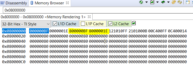
I cannot figure out if access to 0x80000000 when running DDR test from the GEL file is correctly directed to DDR3A.

In my case, what would be the correct configuration sequence (XMC and MSMC) to be sure that read/write to 0x80000000 is directed to DDR3A chip ?

Thank you.

  • Hi,

    You can look at the below registers from a C66x core:

    The highlighted in yellow means 36-bit physical address 0x8_0000_0000 (this is DDR3A) is mapped to 32-bit logical address 0x8000_0000. The mapping size is 2GB. Detailed decoding can be found at: http://www.ti.com/lit/ug/sprugw0c/sprugw0c.pdf  7.3 XMC Memory Protection and Address eXtension (MPAX).

    This is the default value when DSP out of reset (from the same document):

    The XMC configures MPAX segments 0 and 1 so that C66x CorePac can access system memory. The power up configuration is that segment 1 remaps 8000_0000 – FFFF_FFFF in C66x CorePac’s address space to 8:0000_0000 – 8:7FFF_FFFF in the system address map. This corresponds to the first 2GB of address space dedicated to EMIF by the MSMC controller

    Regards, Eric

  • Thanks for the reply.
    I correctly see the values above when I connect to C66xx_0.
    Sorry, but I forget to mention in the initial question that my GEL file is run on ARM 0.
    And my question is how to remap ARM 0 address 0x80000000 to DDR3A.
    Regards.
    Didier.
  • Didier,

    From the K2H data sheet www.ti.com/.../66ak2h14.pdf. 8.1 Memory Map Summary for 66AK2Hxx

    ARM view
    (3) This region is mapped to DDR3B. It is aliased of 00 8000 0000 to 00 9FFF FFFF (the first 512MB of DDR3B) if the state of
    DDR3A_REMAP_EN pin at boot time is ‘0’.
    (5) This region is mapped to DDR3A or DDR3B depending on the state of DDR3A_REMAP_EN pin at boot time. If the pin is ‘1’, this region
    is mapped to the first 2GB of DDR3A which is aliased of 08 0000 0000 to 08 7FFF FFFF. If the pin is ‘0’, this region is mapped as 2GB
    of DDR3B.

    So, from 00 8000 0000 to 00 FFFF FFFF with size 2G is for DDR3B only as viewed from ARM (when you run the GEL from ARM), if DDR3A_REMAP_EN = 0.

    You need to change DDR3A_REMAP_EN = 1 if you want to use ARM to access DDR3A from 0x8000_0000.

    Regards, Eric
  • Hi Eric,

    So, does your answer mean that if DDR3A_REMAP_EN=0 it is impossible to remap 0x80000000 to DDR3A in GEL file ?

    And that there is no possibility to write/read to DDR3A at all ?

    The above 2 questions concern GEL file.

    They also apply for u-boot and Linux.

    Regards.

    Didier.

  • Hello Didier,

    From an ARM point of view, DDR3A_REMAP_EN selects which DDR interface does show up at 0x8000 0000. If you have DDR3_REMAP_EN=0, you will find DDR3B at this address. Please change to DDR3_REMAP_EN=1 if you like to have DDR3A showing up at 0x8000 0000.

    There is another memory range starting at 0x08 0000 0000. Here you will always find DDR3A. From the ARM and also from the DSP view. Please see Table 8-1 in the datasheet for more details:

    Best regards,
      Robert

  • Hi Robert,

    I perfectly understand the DDR3A_REMAP_EN issue. And I don´t absolutely want to see DDR3A at 0x8000_0000.
    I also read the memory map table several times and I understand that DDR3A is available at 0x8_0000_0000.

    If I post this thread this is because I don´t understand clearly how to access the DDR3A from the GEL file.

    DDR3A_REMAP_EN=0 is hardware connected, so I must do with that.

    Question 1 : in GEL file it is not possible to remap 0x8_0000_0000 to a 32bits address. Correct ?

    Question 2 : If I read 4 32bits words beginning at 0x8_0000_0000 I also read the same values if I read from 0x0000_0000 as if the upper "8" in the address is ignored. Can we use 36bits address in a GEL file ?

    Here is my MPAX configuration :

    /*--------------------------------------------------------------*/
    /* xmc_setup() */
    /* XMC MPAX register setting to access DDR3 config space */
    /*--------------------------------------------------------------*/

    //-- !!!!!!!!!!!!!!!!!!!!!!!!!!!!!!!
    //-- See C66x DSP CorePac User Guide
    //-- Figure 7-10 Memory Map Reset Status
    //-- !!!!!!!!!!!!!!!!!!!!!!!!!!!!!!!
    //--
    //-- This is segment 2 (16 segments all)
    //-- (Segments 0 and 1 already enabled at reset)
    #define XMC_BASE_ADDR (0x08000000)
    #define XMPAX2_L (*(int*)(XMC_BASE_ADDR + 0x00000010))
    #define XMPAX2_H (*(int*)(XMC_BASE_ADDR + 0x00000014))
    #define XMPAX3_L (*(int*)(XMC_BASE_ADDR + 0x00000018))
    #define XMPAX3_H (*(int*)(XMC_BASE_ADDR + 0x0000001C))

    xmc_setup()
    {
    /* mapping for ddr emif registers XMPAX*2 */
    // Size = 512 bytes

    //-- RADDR (Replacement address) = 0x121010
    //-- PERM (Permissions) = 0x3F -> Supervisor and user modes can read/write/execute
    // Change PERM from 0xFF to 0x3F, since bits 6-7 are reserved and should be written as 0
    XMPAX2_L = 0x1210103F; /* replacement addr + perm */

    //-- BADDR (Base address) = 0x21010
    //-- SEGSZ (Segment size, 5 bits) = 01011 = 0xB -> 4KB (This is the minimum)
    XMPAX2_H = 0x2101000B; /* base addr + seg size */

    GEL_TextOut("XMC setup complete.\n");
    }

    Question 3 : is it correct ?

    Question 4 : do I need to configure something in MSMC ? I have tried to do something with this MSMC, but without success.

    Here is an extract of my test code.

    #define DDR3A_BASE_ADDRESS 0x800000000
    #define DDR3_TEST_START_ADDRESS (*(int*)(DDR3A_BASE_ADDRESS))

    hotmenu my_ddr3_memory_test ()
    {
    unsigned int read_value_1;
    unsigned int read_value_2;
    unsigned int read_value_3;

    GEL_TextOut( "DDR3 memory test... writing to 0x800000000\n" );

    DDR3_TEST_START_ADDRESS = 0xAAAAAAAA;
    read_value_1 = DDR3_TEST_START_ADDRESS;
    GEL_TextOut( "Reading once, value = %x\n",,,,, read_value_1);

    read_value_2 = DDR3_TEST_START_ADDRESS;
    GEL_TextOut( "Reading once, value = %x\n",,,,, read_value_2);

    read_value_3 = DDR3_TEST_START_ADDRESS;
    GEL_TextOut( "Reading once, value = %x\n",,,,, read_value_3);

    }

    Question 5 : Is it correct ?

    Best regards.

    Didier.
  • Didier,

    A1. GEL only uses the 32-bit address, it is not possible to access DDR3A when it starts from 0x8_0000_0000. To do that on A15, you need to setup the LPAE (Large Physical Address Extensions) and MMU. This is done in Linux U-boot, but it is not available in GEL.

    A2/A3. The XMC you changed only applies to DSP core, it is not helpful when you want to run from ARM.

    A4/A5: You need LPAE and MMU setup to access that from ARM. I think that are big chunks of code, you need to check how U-boot implement it.

    Regards, Eric