This thread has been locked.

If you have a related question, please click the "Ask a related question" button in the top right corner. The newly created question will be automatically linked to this question.

TMS320C5505: SAR ADC battery measurements out of tolerance on some boards with respect to majority of boards

Part Number: TMS320C5505

Hi,

We use the SAR ADC with external Vref taken from the 1.3V core supply to measure system battery voltage and obtain some indication of remaining state of charge.

This method, although subject to errors, is ok for the application in mind.

The production boards all use the same SAR ADC for battery voltage measurements and thus far there has been no issue for many years.

However there have been recent production boards showing inconsistent SAR ADC DSP measurements giving slightly out-off tolerance indication of system battery voltage and we cannot understand what could cause this on a certain minority of DSPs on the production boards.

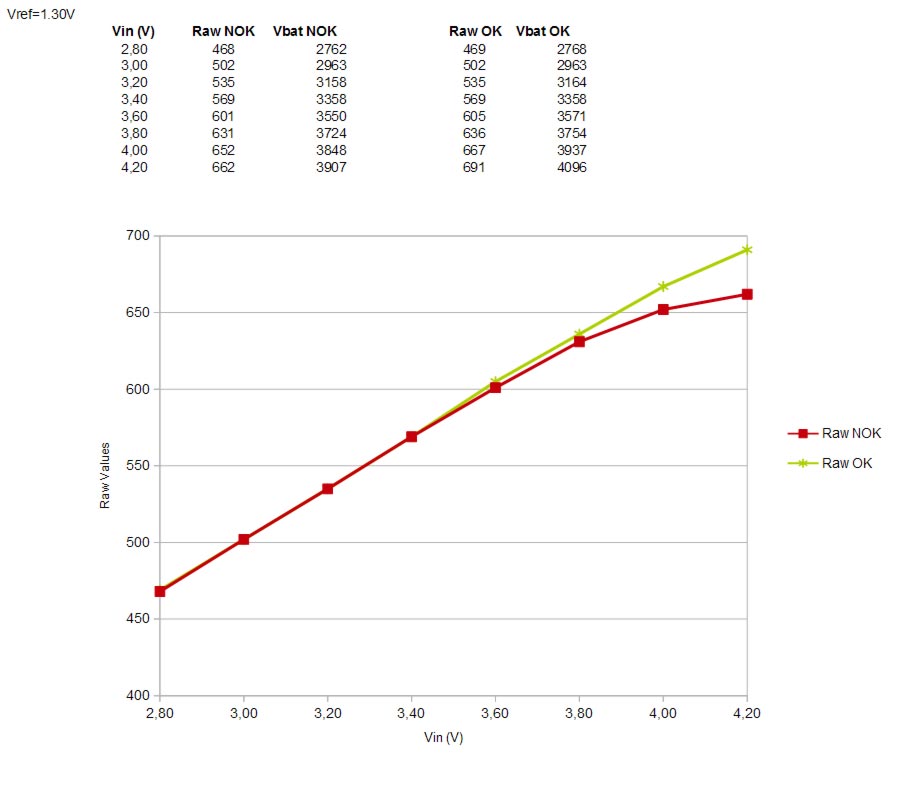
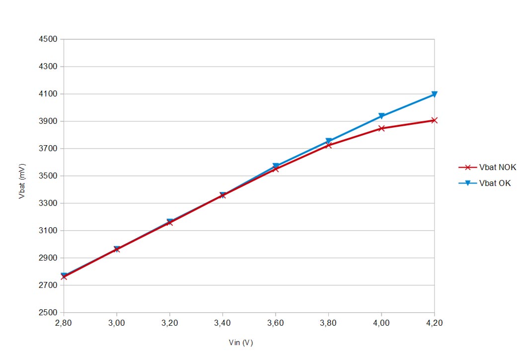
Below there are measurements shown of the input voltage (from a power supply), and the SAR measurement for a production board that we consider "in tolerance" and valid, and one that is "out off tolerance" or invalid/inconsistent, with respect to the majority from previous experience. Measurements done at same temperature.

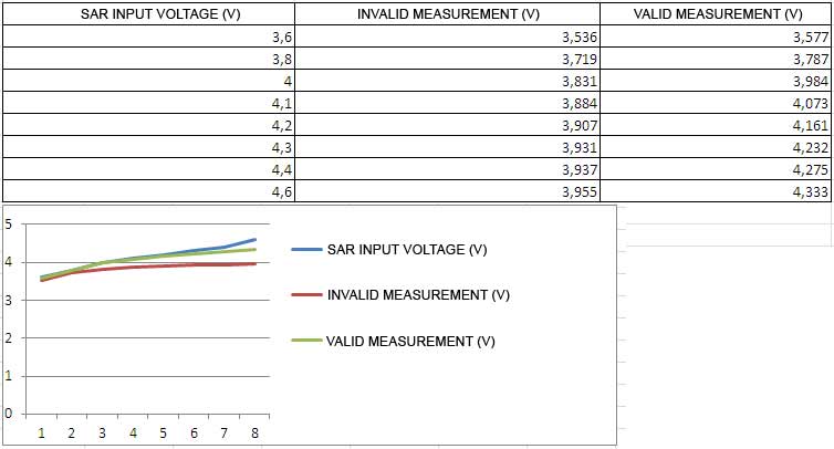
The graphs give a better indication of what goes on. The blue curve is relatively well followed by the green curve up to a value of about 4.4Volts input after which there is some divergence which would not be of concern for a Li-Ion battery system. However the "out-off tolerance" red curve begins diverging at about 3.8V, so earlier than expected, based on all previous experience with 1000+ production boards tested so far.

We are not entirely sure how to explain this even though it is occasional ... As I mentioned before, we are using an external Vcore = 1.3V (+/- 2%) into VDD_ANA and ANA_LDO is not used to avoid loading it beyond its rating. I presume the VDD_ANA input is regulated to an extent however this is not mentioned in the literature. We are not using the internal bandgap references as we required more dynamic range for the battery measurement and 1.3V was available from the Vcore system regulated voltage. However we are open to all ideas if bandgap references would solve this inconsistencies etc.

Would appreciate some suggestions what could cause this occasional inconsistency on some production boards (DSPs). We do not want to consider these boards "required for repair" as we cannot see anything wrong with them otherwise. But there could be some other DSP calibration issue that we either have not taken care off and shows only very occasionally on some DSPs and thus on some production boards.

Regards, citizen

  • Hi citizen,


    Do you have an external resistor divider or some logic between the SAR_ADC input pin and the voltage input/ battery? The GPAIN0 pin is rated upto 3.6V. Others to VDDA_ANA + 0.3V.  The invalid measurement appears to saturate around 6V on the invalid measurement.

    Are you are using GPAIN0 with the internal voltage divider, selecting CH1 and GNDSWON to enable the divider?
    Can you read out the raw 10-bit SAR ADC inputs while probing the voltage at the GPAIN input pin?

    How do you perform voltage calibration for the SAR inputs?

    I do not believe VDD_ANA is regulated internally. Do have decoupling and bulk capacitors? You could probe it with each board for comparison.

    I typically do not recommend using the internal 0.8V and 1.0V SAR ADC references because you cannot route them outside of the device to measure them and calibrate the measurements.

    Hope this helps,
    Mark

  • Hi Mark,

    Yes there is a 50K // 182K divider to lower battery voltage within the GPAIN0 limits by about a factor of 0.215.

    My excuse for the quick measurements. The X-scale refers to the points in the table, so row #6 = 3.931 Volts in the table at 4.3V input (somebody else took the measurements).

    Yes at this point the value seems to start saturating... This results in a "battery full" indication under-measured and "under-indicated" ...


    Are you are using GPAIN0 with the internal voltage divider, selecting CH1 and GNDSWON to enable the divider?

    No need to reduce voltage further as full scale is Vin = 4.2 Volts, which is 0.903 Volts after division.

    Can you read out the raw 10-bit SAR ADC inputs while probing the voltage at the GPAIN input pin?

    How do you perform voltage calibration for the SAR inputs?

    This I'll need to take a look at but I think voltage calibration is done as recommended in the datasheet.

    I do not believe VDD_ANA is regulated internally. Do have decoupling and bulk capacitors? You could probe it with each board for comparison.

    Ok, our 1.3Volts is generated by an LDO with 2% maximum error and there are 10uF input/output caps. The probing I have not done as I did not take the measurements. Will look into this since we could just be at the limits with a particular device with respect to others. However I would have expected the difference to be an offset due to reference voltage difference being constant between two LDO devices regardless of Vinput. Instead there seems to be an early saturation effect at Vinput = 3.7V and then saturation below expected values as per graph.

    I typically do not recommend using the internal 0.8V and 1.0V SAR ADC references because you cannot route them outside of the device to measure them and calibrate the measurements.


    It's OK we weren't using them anyway because of the available 1.3V generated by the onboard LDO

    One thing I may need to look at is the effect of GPAIN0 input leakage current which is specified as ±5μA maximum and how this effects the divided voltage.

    Thanks for the suggestions may need to look at it further when time permits.

    Regards, citizen

  • Thanks citizen,

    The input leakage current might drive you to use different resistor sizes. Are you using precision resistors? You might experiment with debugging/ swapping out resistor divider also.

    When you get a chance, send the SAR ADC registers during a sample. And let me know what ADC output you are reading when it appears to saturate (maybe compare good and bad results).

    Regards,
    Mark

  • Hi Mark,

    So I had a bit of time too look into this a little further and I can confirm the 10-bit raw values duirectly obtained from the software are shown below for thwo different custom boards (one that is out of spec and the one that is as expected and that we've always observed). The raw 10-bit SAR value obtained starts saturating at about Vin-3.6 Volts with respect to the other PCB. This then is scaled to give the mV reading which is also saturated. In both cases the Vref = 1.3V from the LDO, and the voltage divider scale is 49.9K || (49.9K + 182K) = 465 multiplier, so we take (10-bit raw x 13 x 465 ) / 1024 to give us the scaled value in mV.

    So basically I'm bewildered about the possible source of this divergence in SAR value measurements.

    Calibration routine looks something like this below :

    void sar_CalibrateBatteryVoltage(void)
    {
    	// Reset SAR
    	*SARCTRL = 0;
    	// Set GNDON on chanel 0 to find any offset to apply.
    	*SARPINCTRL |= GNDON;
    
    	// Enable the interrupt to make the sar measurement.
    	IRQ_enable(SAR_EVENT);	
    
    	// Make the conversion
    	*SARCTRL = CHSEL_CHANNEL_0 + SAR_START_CONVERT + SNGLCONV_ENABLE;	
    
    	// Wait the semaphore that indicates the end of conversion
    	SEM_pend(&sem_read_battery_level, SYS_FOREVER);
    
    	// Disable the interrupt
    	IRQ_disable(SAR_EVENT);
    
    	// Disable GNDON on chanel 0 to eliminate current draw from the battery.
    	*SARPINCTRL &= ~GNDON;
    }
    

    The actual offset value obtained when running this routine does not seem to be large, and certaily in the order of 1 - 4 (raw value) so about 1 -  2%. Cannot really get enough % to explain saturation at larger end of inputs.

    However I am wondering about the reference of 1.3V LDO we used, as internal references are given of the order of 0.8V and 1.0V, and this probably for a good reason.... We use an external reference of 1.3V and the voltage divider introduces a x0.216 voltage input attenutation factor, but I wonder if this could be the source ?!?

    We would like to have solution in case this ever occurs again (say in the next batch of baords), even though this has been a rare occurance so far ...

    Regards, citizen