This thread has been locked.

If you have a related question, please click the "Ask a related question" button in the top right corner. The newly created question will be automatically linked to this question.

TDA4VM: How to change CSI camera i2c Instance in vision_app?

Part Number: TDA4VM

Hi, Dear Experts :

we setup an "vx_app_single_cam.out" vision_app demo for our customer board.

TDA4EVB use I2C_6 bus for CSI0/CSI1 camera setting.

but we modify our board use I2C_3(CSI0) / I2C_6(CSI1) for camera init, code revise as below :

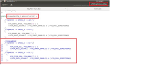
pdk / package / ti /src /device / fpd / ds90ub960.c

void Board_fpdU960GetI2CAddr(uint8_t *chNum,
                             uint8_t *i2cAddr,
                             uint32_t csiInst)
{

     //Gibbs
    if (csiInst == BOARD_CSI_INST_0)
    {
        //*chNum = 6U;          //original EVB
        //*i2cAddr = 0x3DU;     //original EVB
        *chNum = 3U;            //Our Customer Board
        *i2cAddr = 0x3DU;       //Our Customer Board
    }
    else if (csiInst == BOARD_CSI_INST_1)
    {
        //*chNum = 6U;          //original EVB
        //*i2cAddr = 0x36U;     //original EVB
        *chNum = 6U;            //Our Customer Board
        *i2cAddr = 0x3DU;       //Our Customer Board       
    }
    else
    {
        *chNum = 0U;
        *i2cAddr = 0U;
    }
}

We think it's correct setting, but it doesn't work? Does anything missing?

besides this code, do we also need to revise "'k3-j721e-vision-apps.dtbo" ? where is k3-j721e-vision-apps.dtsi ?

Many Thanks

Gibbs


  • The change looks correct from a SW point of view.

  • Hi Mayank:

    Gibbs is my customer.

    some questions:

        A. If they modify the PDK i2C, do they need to modify the Linux DTSI and generate the DTBO for the I2C_3 as well?

            Please confirm.

        B. Do we have the document to address how to generate the DTBO?

    THanks.

    BR Rio

  • Dear Experts :

    Follow previous discussion, I make some update :

    1.  Hardware, csi0, I2C3_SCL / I2C3_SDA ( ) --> MMC2_CK(T26) / MMC2_CMD (T25), the define should be same as EVB

    2.  Hardware, csi1, I2C6_SCL / I2C6_SDA ( ) --> I3C0_SCL (W2) / I3C0_SDA (W1)

    3.  base on new pin define, we generate new  "J721E_pinmux_data.c", and re-build in vision_app

    4.  base on new pin define, we generate new dts "k3-j721e-common-proc-board", and re-build kernel

    but It does not work.

    pls, check appendix files

    Do I miss something?

    Many Thanks.

  • update files.

    7206.J721E_pinmux_data.c
    /**
    * Note: This file was auto-generated by TI PinMux on 5/10/2019 at 3:40:37 PM.
    *
    * \file  J721E_pinmux_data.c
    *
    * \brief  This file contains the pin mux configurations for the boards.
    *         These are prepared based on how the peripherals are extended on
    *         the boards.
    *
    * \copyright Copyright (CU) 2019 Texas Instruments Incorporated -
    *             http://www.ti.com/
    */
    
    /* ========================================================================== */
    /*                             Include Files                                  */
    /* ========================================================================== */
    
    #include "J721E_pinmux.h"
    
    /** Peripheral Pin Configurations */
    
    
    static pinmuxPerCfg_t gDebugss0PinCfg[] =
    {
        /* MyDEBUG1 -> TDI -> V1 */
        {
            PIN_TDI, PIN_MODE(0) | \
            ((PIN_PULL_DISABLE | PIN_INPUT_ENABLE) & (~PIN_PULL_DIRECTION))
        },
        /* MyDEBUG1 -> TDO -> V3 */
        {
            PIN_TDO, PIN_MODE(0) | \
            ((PIN_PULL_DISABLE) & (~PIN_PULL_DIRECTION & ~PIN_INPUT_ENABLE))
        },
        /* MyDEBUG1 -> TMS -> V2 */
        {
            PIN_TMS, PIN_MODE(0) | \
            ((PIN_PULL_DISABLE | PIN_INPUT_ENABLE) & (~PIN_PULL_DIRECTION))
        },
        {PINMUX_END}
    };
    
    static pinmuxModuleCfg_t gDebugssPinCfg[] =
    {
        {0, TRUE, gDebugss0PinCfg},
        {PINMUX_END}
    };
    
    
    static pinmuxPerCfg_t gDp0PinCfg[] =
    {
        /* MyDP0 -> DP0_HPD -> Y4 */
        {
            PIN_SPI0_CS1, PIN_MODE(5) | \
            ((PIN_PULL_DISABLE | PIN_INPUT_ENABLE) & (~PIN_PULL_DIRECTION))
        },
        {PINMUX_END}
    };
    
    static pinmuxModuleCfg_t gDpPinCfg[] =
    {
        {0, TRUE, gDp0PinCfg},
        {PINMUX_END}
    };
    
    
    static pinmuxPerCfg_t gGpio0PinCfg[] =
    {
        /* MySYSTEM1 -> GPIO0_0 -> AC18 */
        {
            PIN_EXTINTN, PIN_MODE(7) | \
            ((PIN_PULL_DISABLE | PIN_INPUT_ENABLE) & (~PIN_PULL_DIRECTION))
        },
        /* MyGPIO0 -> GPIO0_97 -> Y28 */
        {
            PIN_RGMII6_TX_CTL, PIN_MODE(7) | \
            ((PIN_PULL_DISABLE | PIN_INPUT_ENABLE) & (~PIN_PULL_DIRECTION))
        },
        /* MyGPIO0 -> GPIO0_98 -> V23 */
        {
            PIN_RGMII6_RX_CTL, PIN_MODE(7) | \
            ((PIN_PULL_DISABLE | PIN_INPUT_ENABLE) & (~PIN_PULL_DIRECTION))
        },
        /* MyGPIO0 -> GPIO0_117 -> W4 */
        {
            PIN_SPI1_CS1, PIN_MODE(7) | \
            ((PIN_PULL_DISABLE | PIN_INPUT_ENABLE) & (~PIN_PULL_DIRECTION))
        },
        /* MyGPIO0 -> GPIO0_127 -> AC4 */
        {
            PIN_UART1_CTSN, PIN_MODE(7) | \
            ((PIN_PULL_DISABLE | PIN_INPUT_ENABLE) & (~PIN_PULL_DIRECTION))
        },
        {PINMUX_END}
    };
    
    static pinmuxPerCfg_t gGpio1PinCfg[] =
    {
        /* MyGPIO1 -> GPIO1_0 -> AD5 */
        {
            PIN_UART1_RTSN, PIN_MODE(7) | \
            ((PIN_PULL_DISABLE | PIN_INPUT_ENABLE) & (~PIN_PULL_DIRECTION))
        },
        /* MyGPIO1 -> GPIO1_3 -> W3 */
        {
            PIN_MCAN1_RX, PIN_MODE(7) | \
            ((PIN_PULL_DISABLE | PIN_INPUT_ENABLE) & (~PIN_PULL_DIRECTION))
        },
        /* MyGPIO1 -> GPIO1_5 -> W2 */
        {
            PIN_I3C0_SCL, PIN_MODE(7) | \
            ((PIN_PULL_DISABLE | PIN_INPUT_ENABLE) & (~PIN_PULL_DIRECTION))
        },
        /* MyGPIO1 -> GPIO1_6 -> W1 */
        {
            PIN_I3C0_SDA, PIN_MODE(7) | \
            ((PIN_PULL_DISABLE | PIN_INPUT_ENABLE) & (~PIN_PULL_DIRECTION))
        },
        /* MyGPIO1 -> GPIO1_11 -> U2 */
        {
            PIN_ECAP0_IN_APWM_OUT, PIN_MODE(7) | \
            ((PIN_PULL_DISABLE | PIN_INPUT_ENABLE) & (~PIN_PULL_DIRECTION))
        },
        /* MyGPIO1 -> GPIO1_12 -> U3 */
        {
            PIN_EXT_REFCLK1, PIN_MODE(7) | \
            ((PIN_PULL_DISABLE | PIN_INPUT_ENABLE) & (~PIN_PULL_DIRECTION))
        },
        /* MyGPIO1 -> GPIO1_22 -> R28 */
        {
            PIN_MMC1_SDWP, PIN_MODE(7) | \
            ((PIN_PULL_DISABLE | PIN_INPUT_ENABLE) & (~PIN_PULL_DIRECTION))
        },
        /* MyGPIO1 -> GPIO1_23 -> T28 */
        {
            PIN_MMC2_DAT3, PIN_MODE(7) | \
            ((PIN_PULL_DISABLE | PIN_INPUT_ENABLE) & (~PIN_PULL_DIRECTION))
        },
        /* MyGPIO1 -> GPIO1_24 -> T29 */
        {
            PIN_MMC2_DAT2, PIN_MODE(7) | \
            ((PIN_PULL_DISABLE | PIN_INPUT_ENABLE) & (~PIN_PULL_DIRECTION))
        },
        /* MyGPIO1 -> GPIO1_25 -> T27 */
        {
            PIN_MMC2_DAT1, PIN_MODE(7) | \
            ((PIN_PULL_DISABLE | PIN_INPUT_ENABLE) & (~PIN_PULL_DIRECTION))
        },
        /* MyGPIO1 -> GPIO1_26 -> T24 */
        {
            PIN_MMC2_DAT0, PIN_MODE(7) | \
            ((PIN_PULL_DISABLE | PIN_INPUT_ENABLE) & (~PIN_PULL_DIRECTION))
        },
        {PINMUX_END}
    };
    
    static pinmuxModuleCfg_t gGpioPinCfg[] =
    {
        {0, TRUE, gGpio0PinCfg},
        {1, TRUE, gGpio1PinCfg},
        {PINMUX_END}
    };
    
    
    static pinmuxPerCfg_t gI2c2PinCfg[] =
    {
        /* MyI2C2 -> I2C2_SCL -> AA1 */
        {
            PIN_SPI0_CLK, PIN_MODE(2) | \
            ((PIN_PULL_DIRECTION | PIN_INPUT_ENABLE) & (~PIN_PULL_DISABLE))
        },
        /* MyI2C2 -> I2C2_SDA -> AB5 */
        {
            PIN_SPI0_D0, PIN_MODE(2) | \
            ((PIN_PULL_DIRECTION | PIN_INPUT_ENABLE) & (~PIN_PULL_DISABLE))
        },
        {PINMUX_END}
    };
    
    //Gibbs@20210317
    //static pinmuxPerCfg_t gI2c6PinCfg[] =
    //{
        /* MyI2C6 -> I2C6_SCL -> AA3 */
    //    {
    //        PIN_SPI0_D1, PIN_MODE(2) | \
    //        ((PIN_PULL_DIRECTION | PIN_INPUT_ENABLE) & (~PIN_PULL_DISABLE))
    //    },
        /* MyI2C6 -> I2C6_SDA -> Y2 */
    //    {
    //        PIN_SPI1_D1, PIN_MODE(2) | \
    //        ((PIN_PULL_DIRECTION | PIN_INPUT_ENABLE) & (~PIN_PULL_DISABLE))
    //    },
    //    {PINMUX_END}
    //};
    
    //Gibbs@20210317
    static pinmuxPerCfg_t gI2c6PinCfg[] =
    {
        /* MyI2C6 -> I2C6_SCL -> W2 */
        {
            PIN_I3C0_SCL, PIN_MODE(4) | \
            ((PIN_PULL_DIRECTION | PIN_INPUT_ENABLE) & (~PIN_PULL_DISABLE))
        },
        /* MyI2C6 -> I2C6_SDA -> W1 */
        {
            PIN_I3C0_SDA, PIN_MODE(4) | \
            ((PIN_PULL_DIRECTION | PIN_INPUT_ENABLE) & (~PIN_PULL_DISABLE))
        },
        {PINMUX_END}
    };
    
    
    static pinmuxPerCfg_t gI2c0PinCfg[] =
    {
        /* MyI2C0 -> I2C0_SCL -> AC5 */
        {
            PIN_I2C0_SCL, PIN_MODE(0) | \
            ((PIN_PULL_DIRECTION | PIN_INPUT_ENABLE) & (~PIN_PULL_DISABLE))
        },
        /* MyI2C0 -> I2C0_SDA -> AA5 */
        {
            PIN_I2C0_SDA, PIN_MODE(0) | \
            ((PIN_PULL_DIRECTION | PIN_INPUT_ENABLE) & (~PIN_PULL_DISABLE))
        },
        {PINMUX_END}
    };
    
    static pinmuxPerCfg_t gI2c1PinCfg[] =
    {
        /* MyI2C1 -> I2C1_SCL -> Y6 */
        {
            PIN_I2C1_SCL, PIN_MODE(0) | \
            ((PIN_PULL_DIRECTION | PIN_INPUT_ENABLE) & (~PIN_PULL_DISABLE))
        },
        /* MyI2C1 -> I2C1_SDA -> AA6 */
        {
            PIN_I2C1_SDA, PIN_MODE(0) | \
            ((PIN_PULL_DIRECTION | PIN_INPUT_ENABLE) & (~PIN_PULL_DISABLE))
        },
        {PINMUX_END}
    };
    
    static pinmuxPerCfg_t gI2c3PinCfg[] =
    {
        /* MyI2C3 -> I2C3_SCL -> T26 */
        {
            PIN_MMC2_CLK, PIN_MODE(4) | \
            ((PIN_PULL_DIRECTION | PIN_INPUT_ENABLE) & (~PIN_PULL_DISABLE))
        },
        /* MyI2C3 -> I2C3_SDA -> T25 */
        {
            PIN_MMC2_CMD, PIN_MODE(4) | \
            ((PIN_PULL_DIRECTION | PIN_INPUT_ENABLE) & (~PIN_PULL_DISABLE))
        },
        {PINMUX_END}
    };
    
    static pinmuxModuleCfg_t gI2cPinCfg[] =
    {
        {2, TRUE, gI2c2PinCfg},
        {6, TRUE, gI2c6PinCfg},
        {0, TRUE, gI2c0PinCfg},
        {1, TRUE, gI2c1PinCfg},
        {3, TRUE, gI2c3PinCfg},
        {PINMUX_END}
    };
    
    
    static pinmuxPerCfg_t gMcan2PinCfg[] =
    {
        /* MyMCAN2 -> MCAN2_RX -> AC2 */
        {
            PIN_UART0_CTSN, PIN_MODE(3) | \
            ((PIN_PULL_DISABLE | PIN_INPUT_ENABLE) & (~PIN_PULL_DIRECTION))
        },
        /* MyMCAN2 -> MCAN2_TX -> AB1 */
        {
            PIN_UART0_RTSN, PIN_MODE(3) | \
            ((PIN_PULL_DISABLE) & (~PIN_PULL_DIRECTION & ~PIN_INPUT_ENABLE))
        },
        {PINMUX_END}
    };
    
    static pinmuxPerCfg_t gMcan0PinCfg[] =
    {
        /* MyMCAN0 -> MCAN0_RX -> W5 */
        {
            PIN_MCAN0_RX, PIN_MODE(0) | \
            ((PIN_PULL_DISABLE | PIN_INPUT_ENABLE) & (~PIN_PULL_DIRECTION))
        },
        /* MyMCAN0 -> MCAN0_TX -> W6 */
        {
            PIN_MCAN0_TX, PIN_MODE(0) | \
            ((PIN_PULL_DISABLE) & (~PIN_PULL_DIRECTION & ~PIN_INPUT_ENABLE))
        },
        {PINMUX_END}
    };
    
    static pinmuxModuleCfg_t gMcanPinCfg[] =
    {
        {2, TRUE, gMcan2PinCfg},
        {0, TRUE, gMcan0PinCfg},
        {PINMUX_END}
    };
    
    
    static pinmuxPerCfg_t gMcu_i2c0PinCfg[] =
    {
        /* MyMCU_I2C0 -> MCU_I2C0_SCL -> J26 */
        {
            PIN_MCU_I2C0_SCL, PIN_MODE(0) | \
            ((PIN_PULL_DISABLE | PIN_INPUT_ENABLE) & (~PIN_PULL_DIRECTION))
        },
        /* MyMCU_I2C0 -> MCU_I2C0_SDA -> H25 */
        {
            PIN_MCU_I2C0_SDA, PIN_MODE(0) | \
            ((PIN_PULL_DISABLE | PIN_INPUT_ENABLE) & (~PIN_PULL_DIRECTION))
        },
        {PINMUX_END}
    };
    
    static pinmuxModuleCfg_t gMcu_i2cPinCfg[] =
    {
        {0, TRUE, gMcu_i2c0PinCfg},
        {PINMUX_END}
    };
    
    
    static pinmuxPerCfg_t gMcu_i3c0PinCfg[] =
    {
        /* MyMCU_I3C0 -> MCU_I3C0_SCL -> D26 */
        {
            PIN_MCU_I3C0_SCL, PIN_MODE(0) | \
            ((PIN_PULL_DISABLE | PIN_INPUT_ENABLE) & (~PIN_PULL_DIRECTION))
        },
        /* MyMCU_I3C0 -> MCU_I3C0_SDA -> D25 */
        {
            PIN_MCU_I3C0_SDA, PIN_MODE(0) | \
            ((PIN_PULL_DISABLE | PIN_INPUT_ENABLE) & (~PIN_PULL_DIRECTION))
        },
        /* MyMCU_I3C0 -> MCU_I3C0_SDAPULLEN -> E26 */
        {
            PIN_PMIC_POWER_EN0, PIN_MODE(0) | \
            ((PIN_PULL_DISABLE) & (~PIN_PULL_DIRECTION & ~PIN_INPUT_ENABLE))
        },
        {PINMUX_END}
    };
    
    static pinmuxModuleCfg_t gMcu_i3cPinCfg[] =
    {
        {0, TRUE, gMcu_i3c0PinCfg},
        {PINMUX_END}
    };
    
    
    static pinmuxPerCfg_t gMcu_mcan0PinCfg[] =
    {
        /* MyMCU_MCAN0 -> MCU_MCAN0_RX -> C29 */
        {
            PIN_MCU_MCAN0_RX, PIN_MODE(0) | \
            ((PIN_PULL_DISABLE | PIN_INPUT_ENABLE) & (~PIN_PULL_DIRECTION))
        },
        /* MyMCU_MCAN0 -> MCU_MCAN0_TX -> D29 */
        {
            PIN_MCU_MCAN0_TX, PIN_MODE(0) | \
            ((PIN_PULL_DISABLE) & (~PIN_PULL_DIRECTION & ~PIN_INPUT_ENABLE))
        },
        {PINMUX_END}
    };
    
    static pinmuxPerCfg_t gMcu_mcan1PinCfg[] =
    {
        /* MyMCU_MCAN1 -> MCU_MCAN1_RX -> G24 */
        {
            PIN_WKUP_GPIO0_5, PIN_MODE(0) | \
            ((PIN_PULL_DISABLE | PIN_INPUT_ENABLE) & (~PIN_PULL_DIRECTION))
        },
        /* MyMCU_MCAN1 -> MCU_MCAN1_TX -> G25 */
        {
            PIN_WKUP_GPIO0_4, PIN_MODE(0) | \
            ((PIN_PULL_DISABLE) & (~PIN_PULL_DIRECTION & ~PIN_INPUT_ENABLE))
        },
        {PINMUX_END}
    };
    
    static pinmuxModuleCfg_t gMcu_mcanPinCfg[] =
    {
        {0, TRUE, gMcu_mcan0PinCfg},
        {1, TRUE, gMcu_mcan1PinCfg},
        {PINMUX_END}
    };
    
    
    static pinmuxPerCfg_t gMcu_mdio0PinCfg[] =
    {
        /* MyMCU_MDIO1 -> MCU_MDIO0_MDC -> F23 */
        {
            PIN_MCU_MDIO0_MDC, PIN_MODE(0) | \
            ((PIN_PULL_DISABLE) & (~PIN_PULL_DIRECTION & ~PIN_INPUT_ENABLE))
        },
        /* MyMCU_MDIO1 -> MCU_MDIO0_MDIO -> E23 */
        {
            PIN_MCU_MDIO0_MDIO, PIN_MODE(0) | \
            ((PIN_PULL_DISABLE | PIN_INPUT_ENABLE) & (~PIN_PULL_DIRECTION))
        },
        {PINMUX_END}
    };
    
    static pinmuxModuleCfg_t gMcu_mdioPinCfg[] =
    {
        {0, TRUE, gMcu_mdio0PinCfg},
        {PINMUX_END}
    };
    
    
    static pinmuxPerCfg_t gMcu_fss0_ospi0PinCfg[] =
    {
        /* MyMCU_OSPI0 -> MCU_OSPI0_CLK -> E20 */
        {
            PIN_MCU_OSPI0_CLK, PIN_MODE(0) | \
            ((PIN_PULL_DISABLE) & (~PIN_PULL_DIRECTION & ~PIN_INPUT_ENABLE))
        },
        /* MyMCU_OSPI0 -> MCU_OSPI0_CSn0 -> F19 */
        {
            PIN_MCU_OSPI0_CSN0, PIN_MODE(0) | \
            ((PIN_PULL_DISABLE) & (~PIN_PULL_DIRECTION & ~PIN_INPUT_ENABLE))
        },
        /* MyMCU_OSPI0 -> MCU_OSPI0_D0 -> D20 */
        {
            PIN_MCU_OSPI0_D0, PIN_MODE(0) | \
            ((PIN_PULL_DISABLE | PIN_INPUT_ENABLE) & (~PIN_PULL_DIRECTION))
        },
        /* MyMCU_OSPI0 -> MCU_OSPI0_D1 -> G19 */
        {
            PIN_MCU_OSPI0_D1, PIN_MODE(0) | \
            ((PIN_PULL_DISABLE | PIN_INPUT_ENABLE) & (~PIN_PULL_DIRECTION))
        },
        /* MyMCU_OSPI0 -> MCU_OSPI0_D2 -> G20 */
        {
            PIN_MCU_OSPI0_D2, PIN_MODE(0) | \
            ((PIN_PULL_DISABLE | PIN_INPUT_ENABLE) & (~PIN_PULL_DIRECTION))
        },
        /* MyMCU_OSPI0 -> MCU_OSPI0_D3 -> F20 */
        {
            PIN_MCU_OSPI0_D3, PIN_MODE(0) | \
            ((PIN_PULL_DISABLE | PIN_INPUT_ENABLE) & (~PIN_PULL_DIRECTION))
        },
        /* MyMCU_OSPI0 -> MCU_OSPI0_D4 -> F21 */
        {
            PIN_MCU_OSPI0_D4, PIN_MODE(0) | \
            ((PIN_PULL_DISABLE | PIN_INPUT_ENABLE) & (~PIN_PULL_DIRECTION))
        },
        /* MyMCU_OSPI0 -> MCU_OSPI0_D5 -> E21 */
        {
            PIN_MCU_OSPI0_D5, PIN_MODE(0) | \
            ((PIN_PULL_DISABLE | PIN_INPUT_ENABLE) & (~PIN_PULL_DIRECTION))
        },
        /* MyMCU_OSPI0 -> MCU_OSPI0_D6 -> B22 */
        {
            PIN_MCU_OSPI0_D6, PIN_MODE(0) | \
            ((PIN_PULL_DISABLE | PIN_INPUT_ENABLE) & (~PIN_PULL_DIRECTION))
        },
        /* MyMCU_OSPI0 -> MCU_OSPI0_D7 -> G21 */
        {
            PIN_MCU_OSPI0_D7, PIN_MODE(0) | \
            ((PIN_PULL_DISABLE | PIN_INPUT_ENABLE) & (~PIN_PULL_DIRECTION))
        },
        /* MyMCU_OSPI0 -> MCU_OSPI0_DQS -> D21 */
        {
            PIN_MCU_OSPI0_DQS, PIN_MODE(0) | \
            ((PIN_PULL_DISABLE | PIN_INPUT_ENABLE) & (~PIN_PULL_DIRECTION))
        },
        {PINMUX_END}
    };
    
    static pinmuxPerCfg_t gMcu_fss0_ospi1PinCfg[] =
    {
        /* MyMCU_OSPI1 -> MCU_OSPI1_CLK -> F22 */
        {
            PIN_MCU_OSPI1_CLK, PIN_MODE(0) | \
            ((PIN_PULL_DISABLE) & (~PIN_PULL_DIRECTION & ~PIN_INPUT_ENABLE))
        },
        /* MyMCU_OSPI1 -> MCU_OSPI1_CSn0 -> C22 */
        {
            PIN_MCU_OSPI1_CSN0, PIN_MODE(0) | \
            ((PIN_PULL_DISABLE) & (~PIN_PULL_DIRECTION & ~PIN_INPUT_ENABLE))
        },
        /* MyMCU_OSPI1 -> MCU_OSPI1_D0 -> D22 */
        {
            PIN_MCU_OSPI1_D0, PIN_MODE(0) | \
            ((PIN_PULL_DISABLE | PIN_INPUT_ENABLE) & (~PIN_PULL_DIRECTION))
        },
        /* MyMCU_OSPI1 -> MCU_OSPI1_D1 -> G22 */
        {
            PIN_MCU_OSPI1_D1, PIN_MODE(0) | \
            ((PIN_PULL_DISABLE | PIN_INPUT_ENABLE) & (~PIN_PULL_DIRECTION))
        },
        /* MyMCU_OSPI1 -> MCU_OSPI1_D2 -> D23 */
        {
            PIN_MCU_OSPI1_D2, PIN_MODE(0) | \
            ((PIN_PULL_DISABLE | PIN_INPUT_ENABLE) & (~PIN_PULL_DIRECTION))
        },
        /* MyMCU_OSPI1 -> MCU_OSPI1_D3 -> C23 */
        {
            PIN_MCU_OSPI1_D3, PIN_MODE(0) | \
            ((PIN_PULL_DISABLE | PIN_INPUT_ENABLE) & (~PIN_PULL_DIRECTION))
        },
        /* MyMCU_OSPI1 -> MCU_OSPI1_DQS -> B23 */
        {
            PIN_MCU_OSPI1_DQS, PIN_MODE(0) | \
            ((PIN_PULL_DISABLE | PIN_INPUT_ENABLE) & (~PIN_PULL_DIRECTION))
        },
        /* MyMCU_OSPI1 -> MCU_OSPI1_LBCLKO -> A23 */
        {
            PIN_MCU_OSPI1_LBCLKO, PIN_MODE(0) | \
            ((PIN_PULL_DISABLE | PIN_INPUT_ENABLE) & (~PIN_PULL_DIRECTION))
        },
        {PINMUX_END}
    };
    
    static pinmuxModuleCfg_t gMcu_fss0_ospiPinCfg[] =
    {
        {0, TRUE, gMcu_fss0_ospi0PinCfg},
        {1, TRUE, gMcu_fss0_ospi1PinCfg},
        {PINMUX_END}
    };
    
    static pinmuxPerCfg_t gMcu_fss0_hpb0PinCfg[] =
    {
        /* MyMCU_FSS0_HPB1 -> MCU_HYPERBUS0_CK -> E20 */
        {
            PIN_MCU_OSPI0_CLK, PIN_MODE(1) | \
            ((PIN_PULL_DISABLE) & (~PIN_PULL_DIRECTION & ~PIN_INPUT_ENABLE))
        },
        /* MyMCU_FSS0_HPB1 -> MCU_HYPERBUS0_CSn0 -> F19 */
        {
            PIN_MCU_OSPI0_CSN0, PIN_MODE(1) | \
            ((PIN_PULL_DISABLE) & (~PIN_PULL_DIRECTION & ~PIN_INPUT_ENABLE))
        },
        /* MyMCU_FSS0_HPB1 -> MCU_HYPERBUS0_DQ0 -> D20 */
        {
            PIN_MCU_OSPI0_D0, PIN_MODE(1) | \
            ((PIN_PULL_DISABLE | PIN_INPUT_ENABLE) & (~PIN_PULL_DIRECTION))
        },
        /* MyMCU_FSS0_HPB1 -> MCU_HYPERBUS0_DQ1 -> G19 */
        {
            PIN_MCU_OSPI0_D1, PIN_MODE(1) | \
            ((PIN_PULL_DISABLE | PIN_INPUT_ENABLE) & (~PIN_PULL_DIRECTION))
        },
        /* MyMCU_FSS0_HPB1 -> MCU_HYPERBUS0_DQ2 -> G20 */
        {
            PIN_MCU_OSPI0_D2, PIN_MODE(1) | \
            ((PIN_PULL_DISABLE | PIN_INPUT_ENABLE) & (~PIN_PULL_DIRECTION))
        },
        /* MyMCU_FSS0_HPB1 -> MCU_HYPERBUS0_DQ3 -> F20 */
        {
            PIN_MCU_OSPI0_D3, PIN_MODE(1) | \
            ((PIN_PULL_DISABLE | PIN_INPUT_ENABLE) & (~PIN_PULL_DIRECTION))
        },
        /* MyMCU_FSS0_HPB1 -> MCU_HYPERBUS0_DQ4 -> F21 */
        {
            PIN_MCU_OSPI0_D4, PIN_MODE(1) | \
            ((PIN_PULL_DISABLE | PIN_INPUT_ENABLE) & (~PIN_PULL_DIRECTION))
        },
        /* MyMCU_FSS0_HPB1 -> MCU_HYPERBUS0_DQ5 -> E21 */
        {
            PIN_MCU_OSPI0_D5, PIN_MODE(1) | \
            ((PIN_PULL_DISABLE | PIN_INPUT_ENABLE) & (~PIN_PULL_DIRECTION))
        },
        /* MyMCU_FSS0_HPB1 -> MCU_HYPERBUS0_DQ6 -> B22 */
        {
            PIN_MCU_OSPI0_D6, PIN_MODE(1) | \
            ((PIN_PULL_DISABLE | PIN_INPUT_ENABLE) & (~PIN_PULL_DIRECTION))
        },
        /* MyMCU_FSS0_HPB1 -> MCU_HYPERBUS0_DQ7 -> G21 */
        {
            PIN_MCU_OSPI0_D7, PIN_MODE(1) | \
            ((PIN_PULL_DISABLE | PIN_INPUT_ENABLE) & (~PIN_PULL_DIRECTION))
        },
        /* MyMCU_FSS0_HPB1 -> MCU_OSPI0_DQS -> D21 */
        {
            PIN_MCU_OSPI0_DQS, PIN_MODE(1) | \
            ((PIN_PULL_DISABLE | PIN_INPUT_ENABLE) & (~PIN_PULL_DIRECTION))
        },
        /* MyMCU_FSS0_HPB1 -> MCU_OSPI0_LBCLKO -> C21 */
        {
            PIN_MCU_OSPI0_LBCLKO, PIN_MODE(1) | \
            ((PIN_PULL_DISABLE | PIN_INPUT_ENABLE) & (~PIN_PULL_DIRECTION))
        },
        {PINMUX_END}
    };
    
    static pinmuxModuleCfg_t gMcu_fss0_hpbPinCfg[] =
    {
        {0, TRUE, gMcu_fss0_hpb0PinCfg},
        {PINMUX_END}
    };
    
    
    static pinmuxPerCfg_t gMcu_rgmii1PinCfg[] =
    {
        /* MyMCU_RGMII1 -> MCU_RGMII1_RD0 -> B24 */
        {
            PIN_MCU_RGMII1_RD0, PIN_MODE(0) | \
            ((PIN_PULL_DISABLE | PIN_INPUT_ENABLE) & (~PIN_PULL_DIRECTION))
        },
        /* MyMCU_RGMII1 -> MCU_RGMII1_RD1 -> A24 */
        {
            PIN_MCU_RGMII1_RD1, PIN_MODE(0) | \
            ((PIN_PULL_DISABLE | PIN_INPUT_ENABLE) & (~PIN_PULL_DIRECTION))
        },
        /* MyMCU_RGMII1 -> MCU_RGMII1_RD2 -> D24 */
        {
            PIN_MCU_RGMII1_RD2, PIN_MODE(0) | \
            ((PIN_PULL_DISABLE | PIN_INPUT_ENABLE) & (~PIN_PULL_DIRECTION))
        },
        /* MyMCU_RGMII1 -> MCU_RGMII1_RD3 -> A25 */
        {
            PIN_MCU_RGMII1_RD3, PIN_MODE(0) | \
            ((PIN_PULL_DISABLE | PIN_INPUT_ENABLE) & (~PIN_PULL_DIRECTION))
        },
        /* MyMCU_RGMII1 -> MCU_RGMII1_RXC -> C24 */
        {
            PIN_MCU_RGMII1_RXC, PIN_MODE(0) | \
            ((PIN_PULL_DISABLE | PIN_INPUT_ENABLE) & (~PIN_PULL_DIRECTION))
        },
        /* MyMCU_RGMII1 -> MCU_RGMII1_RX_CTL -> C25 */
        {
            PIN_MCU_RGMII1_RX_CTL, PIN_MODE(0) | \
            ((PIN_PULL_DISABLE | PIN_INPUT_ENABLE) & (~PIN_PULL_DIRECTION))
        },
        /* MyMCU_RGMII1 -> MCU_RGMII1_TD0 -> B25 */
        {
            PIN_MCU_RGMII1_TD0, PIN_MODE(0) | \
            ((PIN_PULL_DISABLE) & (~PIN_PULL_DIRECTION & ~PIN_INPUT_ENABLE))
        },
        /* MyMCU_RGMII1 -> MCU_RGMII1_TD1 -> A26 */
        {
            PIN_MCU_RGMII1_TD1, PIN_MODE(0) | \
            ((PIN_PULL_DISABLE) & (~PIN_PULL_DIRECTION & ~PIN_INPUT_ENABLE))
        },
        /* MyMCU_RGMII1 -> MCU_RGMII1_TD2 -> A27 */
        {
            PIN_MCU_RGMII1_TD2, PIN_MODE(0) | \
            ((PIN_PULL_DISABLE) & (~PIN_PULL_DIRECTION & ~PIN_INPUT_ENABLE))
        },
        /* MyMCU_RGMII1 -> MCU_RGMII1_TD3 -> A28 */
        {
            PIN_MCU_RGMII1_TD3, PIN_MODE(0) | \
            ((PIN_PULL_DISABLE) & (~PIN_PULL_DIRECTION & ~PIN_INPUT_ENABLE))
        },
        /* MyMCU_RGMII1 -> MCU_RGMII1_TXC -> B26 */
        {
            PIN_MCU_RGMII1_TXC, PIN_MODE(0) | \
            ((PIN_PULL_DISABLE) & (~PIN_PULL_DIRECTION & ~PIN_INPUT_ENABLE))
        },
        /* MyMCU_RGMII1 -> MCU_RGMII1_TX_CTL -> B27 */
        {
            PIN_MCU_RGMII1_TX_CTL, PIN_MODE(0) | \
            ((PIN_PULL_DISABLE) & (~PIN_PULL_DIRECTION & ~PIN_INPUT_ENABLE))
        },
        {PINMUX_END}
    };
    
    static pinmuxModuleCfg_t gMcu_rgmiiPinCfg[] =
    {
        {1, TRUE, gMcu_rgmii1PinCfg},
        {PINMUX_END}
    };
    
    
    static pinmuxPerCfg_t gMcu_uart0PinCfg[] =
    {
        /* MyMCU_UART0 -> MCU_UART0_CTSn -> H29 */
        {
            PIN_WKUP_GPIO0_14, PIN_MODE(0) | \
            ((PIN_PULL_DISABLE | PIN_INPUT_ENABLE) & (~PIN_PULL_DIRECTION))
        },
        /* MyMCU_UART0 -> MCU_UART0_RTSn -> J27 */
        {
            PIN_WKUP_GPIO0_15, PIN_MODE(0) | \
            ((PIN_PULL_DISABLE) & (~PIN_PULL_DIRECTION & ~PIN_INPUT_ENABLE))
        },
        /* MyMCU_UART0 -> MCU_UART0_RXD -> H28 */
        {
            PIN_WKUP_GPIO0_13, PIN_MODE(0) | \
            ((PIN_PULL_DISABLE | PIN_INPUT_ENABLE) & (~PIN_PULL_DIRECTION))
        },
        /* MyMCU_UART0 -> MCU_UART0_TXD -> G29 */
        {
            PIN_WKUP_GPIO0_12, PIN_MODE(0) | \
            ((PIN_PULL_DISABLE) & (~PIN_PULL_DIRECTION & ~PIN_INPUT_ENABLE))
        },
        {PINMUX_END}
    };
    
    static pinmuxModuleCfg_t gMcu_uartPinCfg[] =
    {
        {0, TRUE, gMcu_uart0PinCfg},
        {PINMUX_END}
    };
    
    
    static pinmuxPerCfg_t gMdio0PinCfg[] =
    {
        /* MyMDIO1 -> MDIO0_MDC -> V24 */
        {
            PIN_MDIO0_MDC, PIN_MODE(0) | \
            ((PIN_PULL_DISABLE) & (~PIN_PULL_DIRECTION & ~PIN_INPUT_ENABLE))
        },
        /* MyMDIO1 -> MDIO0_MDIO -> V26 */
        {
            PIN_MDIO0_MDIO, PIN_MODE(0) | \
            ((PIN_PULL_DISABLE | PIN_INPUT_ENABLE) & (~PIN_PULL_DIRECTION))
        },
        {PINMUX_END}
    };
    
    static pinmuxModuleCfg_t gMdioPinCfg[] =
    {
        {0, TRUE, gMdio0PinCfg},
        {PINMUX_END}
    };
    
    
    static pinmuxPerCfg_t gMlb0PinCfg[] =
    {
        /* MyMLB0 -> MLB0_MLBCN -> AE2 */
        {
            PIN_MLB0_MLBCN, PIN_MODE(0) | \
            ((PIN_PULL_DISABLE | PIN_INPUT_ENABLE) & (~PIN_PULL_DIRECTION))
        },
        /* MyMLB0 -> MLB0_MLBCP -> AD2 */
        {
            PIN_MLB0_MLBCP, PIN_MODE(0) | \
            ((PIN_PULL_DISABLE | PIN_INPUT_ENABLE) & (~PIN_PULL_DIRECTION))
        },
        /* MyMLB0 -> MLB0_MLBDN -> AD3 */
        {
            PIN_MLB0_MLBDN, PIN_MODE(0) | \
            ((PIN_PULL_DISABLE) & (~PIN_PULL_DIRECTION & ~PIN_INPUT_ENABLE))
        },
        /* MyMLB0 -> MLB0_MLBDP -> AC3 */
        {
            PIN_MLB0_MLBDP, PIN_MODE(0) | \
            ((PIN_PULL_DISABLE) & (~PIN_PULL_DIRECTION & ~PIN_INPUT_ENABLE))
        },
        /* MyMLB0 -> MLB0_MLBSN -> AC1 */
        {
            PIN_MLB0_MLBSN, PIN_MODE(0) | \
            ((PIN_PULL_DISABLE) & (~PIN_PULL_DIRECTION & ~PIN_INPUT_ENABLE))
        },
        /* MyMLB0 -> MLB0_MLBSP -> AD1 */
        {
            PIN_MLB0_MLBSP, PIN_MODE(0) | \
            ((PIN_PULL_DISABLE) & (~PIN_PULL_DIRECTION & ~PIN_INPUT_ENABLE))
        },
        {PINMUX_END}
    };
    
    static pinmuxModuleCfg_t gMlbPinCfg[] =
    {
        {0, TRUE, gMlb0PinCfg},
        {PINMUX_END}
    };
    
    
    static pinmuxPerCfg_t gMmcsd1PinCfg[] =
    {
        /* MyMMC1 -> MMC1_CLK -> P25 */
        {
            PIN_MMC1_CLK, PIN_MODE(0) | \
            ((PIN_PULL_DIRECTION | PIN_INPUT_ENABLE) & (~PIN_PULL_DISABLE))
        },
        /* MyMMC1 -> MMC1_CMD -> R29 */
        {
            PIN_MMC1_CMD, PIN_MODE(0) | \
            ((PIN_PULL_DIRECTION | PIN_INPUT_ENABLE) & (~PIN_PULL_DISABLE))
        },
        /* MyMMC1 -> MMC1_DAT0 -> R24 */
        {
            PIN_MMC1_DAT0, PIN_MODE(0) | \
            ((PIN_PULL_DIRECTION | PIN_INPUT_ENABLE) & (~PIN_PULL_DISABLE))
        },
        /* MyMMC1 -> MMC1_DAT1 -> P24 */
        {
            PIN_MMC1_DAT1, PIN_MODE(0) | \
            ((PIN_PULL_DIRECTION | PIN_INPUT_ENABLE) & (~PIN_PULL_DISABLE))
        },
        /* MyMMC1 -> MMC1_DAT2 -> R25 */
        {
            PIN_MMC1_DAT2, PIN_MODE(0) | \
            ((PIN_PULL_DIRECTION | PIN_INPUT_ENABLE) & (~PIN_PULL_DISABLE))
        },
        /* MyMMC1 -> MMC1_DAT3 -> R26 */
        {
            PIN_MMC1_DAT3, PIN_MODE(0) | \
            ((PIN_PULL_DIRECTION | PIN_INPUT_ENABLE) & (~PIN_PULL_DISABLE))
        },
        /* MyMMC1 -> MMC1_SDCD -> P23 */
        {
            PIN_MMC1_SDCD, PIN_MODE(0) | \
            ((PIN_PULL_DIRECTION | PIN_INPUT_ENABLE) & (~PIN_PULL_DISABLE))
        },
        /* MyMMC1 -> MMC1_CLKLB */
        {
            PIN_MMC1_CLKLB, PIN_MODE(0) | \
            ((PIN_PULL_DIRECTION | PIN_INPUT_ENABLE) & (~PIN_PULL_DISABLE))
        },
        {PINMUX_END}
    };
    
    static pinmuxModuleCfg_t gMmcsdPinCfg[] =
    {
        {1, TRUE, gMmcsd1PinCfg},
        {PINMUX_END}
    };
    
    
    static pinmuxPerCfg_t gSystem0PinCfg[] =
    {
        /* MySYSTEM1 -> AUDIO_EXT_REFCLK2 -> W26 */
        {
            PIN_RGMII6_RXC, PIN_MODE(3) | \
            ((PIN_PULL_DISABLE | PIN_INPUT_ENABLE) & (~PIN_PULL_DIRECTION))
        },
        /* MySYSTEM1 -> OBSCLK0 -> V5 */
        {
            PIN_TIMER_IO1, PIN_MODE(2) | \
            ((PIN_PULL_DISABLE) & (~PIN_PULL_DIRECTION & ~PIN_INPUT_ENABLE))
        },
        /* MySYSTEM1 -> PORz_OUT -> U1 */
        {
            PIN_PORZ_OUT, PIN_MODE(0) | \
            ((PIN_PULL_DISABLE) & (~PIN_PULL_DIRECTION & ~PIN_INPUT_ENABLE))
        },
        /* MySYSTEM1 -> RESETSTATz -> T6 */
        {
            PIN_RESETSTATZ, PIN_MODE(0) | \
            ((PIN_PULL_DISABLE) & (~PIN_PULL_DIRECTION & ~PIN_INPUT_ENABLE))
        },
        /* MySYSTEM1 -> SOC_SAFETY_ERRORn -> U4 */
        {
            PIN_SOC_SAFETY_ERRORN, PIN_MODE(0) | \
            ((PIN_PULL_DISABLE | PIN_INPUT_ENABLE) & (~PIN_PULL_DIRECTION))
        },
        /* MySYSTEM1 -> SYSCLKOUT0 -> V6 */
        {
            PIN_TIMER_IO0, PIN_MODE(2) | \
            ((PIN_PULL_DISABLE) & (~PIN_PULL_DIRECTION & ~PIN_INPUT_ENABLE))
        },
        {PINMUX_END}
    };
    
    static pinmuxModuleCfg_t gSystemPinCfg[] =
    {
        {0, TRUE, gSystem0PinCfg},
        {PINMUX_END}
    };
    
    
    static pinmuxPerCfg_t gUart4PinCfg[] =
    {
        /* MyUART4 -> UART4_RXD -> W23 */
        {
            PIN_RGMII6_TD3, PIN_MODE(1) | \
            ((PIN_PULL_DISABLE | PIN_INPUT_ENABLE) & (~PIN_PULL_DIRECTION))
        },
        /* MyUART4 -> UART4_TXD -> W28 */
        {
            PIN_RGMII6_TD2, PIN_MODE(1) | \
            ((PIN_PULL_DISABLE) & (~PIN_PULL_DIRECTION & ~PIN_INPUT_ENABLE))
        },
        {PINMUX_END}
    };
    
    static pinmuxPerCfg_t gUart0PinCfg[] =
    {
        /* MyUART0 -> UART0_CTSn -> Y3 */
        {
            PIN_SPI1_CS0, PIN_MODE(1) | \
            ((PIN_PULL_DISABLE | PIN_INPUT_ENABLE) & (~PIN_PULL_DIRECTION))
        },
        /* MyUART0 -> UART0_RTSn -> AA2 */
        {
            PIN_SPI0_CS0, PIN_MODE(1) | \
            ((PIN_PULL_DISABLE) & (~PIN_PULL_DIRECTION & ~PIN_INPUT_ENABLE))
        },
        /* MyUART0 -> UART0_RXD -> AB2 */
        {
            PIN_UART0_RXD, PIN_MODE(0) | \
            ((PIN_PULL_DISABLE | PIN_INPUT_ENABLE) & (~PIN_PULL_DIRECTION))
        },
        /* MyUART0 -> UART0_TXD -> AB3 */
        {
            PIN_UART0_TXD, PIN_MODE(0) | \
            ((PIN_PULL_DISABLE) & (~PIN_PULL_DIRECTION & ~PIN_INPUT_ENABLE))
        },
        {PINMUX_END}
    };
    
    static pinmuxPerCfg_t gUart2PinCfg[] =
    {
        /* MyUART2 -> UART2_RXD -> Y1 */
        {
            PIN_SPI1_CLK, PIN_MODE(3) | \
            ((PIN_PULL_DISABLE | PIN_INPUT_ENABLE) & (~PIN_PULL_DIRECTION))
        },
        /* MyUART2 -> UART2_TXD -> Y5 */
        {
            PIN_SPI1_D0, PIN_MODE(3) | \
            ((PIN_PULL_DISABLE) & (~PIN_PULL_DIRECTION & ~PIN_INPUT_ENABLE))
        },
        {PINMUX_END}
    };
    
    static pinmuxPerCfg_t gUart1PinCfg[] =
    {
        /* MyUART1 -> UART1_RXD -> AA4 */
        {
            PIN_UART1_RXD, PIN_MODE(0) | \
            ((PIN_PULL_DISABLE | PIN_INPUT_ENABLE) & (~PIN_PULL_DIRECTION))
        },
        /* MyUART1 -> UART1_TXD -> AB4 */
        {
            PIN_UART1_TXD, PIN_MODE(0) | \
            ((PIN_PULL_DISABLE) & (~PIN_PULL_DIRECTION & ~PIN_INPUT_ENABLE))
        },
        {PINMUX_END}
    };
    
    static pinmuxModuleCfg_t gUartPinCfg[] =
    {
        {4, TRUE, gUart4PinCfg},
        {0, TRUE, gUart0PinCfg},
        {2, TRUE, gUart2PinCfg},
        {1, TRUE, gUart1PinCfg},
        {PINMUX_END}
    };
    
    
    static pinmuxPerCfg_t gUsb1PinCfg[] =
    {
        /* MyUSB1 -> USB1_DRVVBUS -> V4 */
        {
            PIN_MCAN1_TX, PIN_MODE(4) | \
            ((PIN_PULL_DISABLE) & (~PIN_PULL_DIRECTION & ~PIN_INPUT_ENABLE))
        },
        {PINMUX_END}
    };
    
    static pinmuxPerCfg_t gUsb0PinCfg[] =
    {
        /* MyUSB0 -> USB0_DRVVBUS -> U6 */
        {
            PIN_USB0_DRVVBUS, PIN_MODE(0) | \
            ((PIN_PULL_DISABLE) & (~PIN_PULL_DIRECTION & ~PIN_INPUT_ENABLE))
        },
        {PINMUX_END}
    };
    
    static pinmuxModuleCfg_t gUsbPinCfg[] =
    {
        {1, TRUE, gUsb1PinCfg},
        {0, TRUE, gUsb0PinCfg},
        {PINMUX_END}
    };
    
    
    static pinmuxPerCfg_t gWkup_debugss0PinCfg[] =
    {
        /* MyWKUP_DEBUG -> EMU0 -> C26 */
        {
            PIN_EMU0, PIN_MODE(0) | \
            ((PIN_PULL_DISABLE | PIN_INPUT_ENABLE) & (~PIN_PULL_DIRECTION))
        },
        /* MyWKUP_DEBUG -> EMU1 -> B29 */
        {
            PIN_EMU1, PIN_MODE(0) | \
            ((PIN_PULL_DISABLE | PIN_INPUT_ENABLE) & (~PIN_PULL_DIRECTION))
        },
        /* MyWKUP_DEBUG -> TCK -> E29 */
        {
            PIN_TCK, PIN_MODE(0) | \
            ((PIN_PULL_DISABLE | PIN_INPUT_ENABLE) & (~PIN_PULL_DIRECTION))
        },
        /* MyWKUP_DEBUG -> TRSTn -> F24 */
        {
            PIN_TRSTN, PIN_MODE(0) | \
            ((PIN_PULL_DISABLE | PIN_INPUT_ENABLE) & (~PIN_PULL_DIRECTION))
        },
        {PINMUX_END}
    };
    
    static pinmuxModuleCfg_t gWkup_debugssPinCfg[] =
    {
        {0, TRUE, gWkup_debugss0PinCfg},
        {PINMUX_END}
    };
    
    
    static pinmuxPerCfg_t gWkup_gpio0PinCfg[] =
    {
        /* MyWKUP_GPIO0 -> WKUP_GPIO0_0 -> F26 */
        {
            PIN_WKUP_GPIO0_0, PIN_MODE(7) | \
            ((PIN_PULL_DISABLE | PIN_INPUT_ENABLE) & (~PIN_PULL_DIRECTION))
        },
        /* MyWKUP_GPIO0 -> WKUP_GPIO0_1 -> F25 */
        {
            PIN_WKUP_GPIO0_1, PIN_MODE(7) | \
            ((PIN_PULL_DISABLE | PIN_INPUT_ENABLE) & (~PIN_PULL_DIRECTION))
        },
        /* MyWKUP_GPIO0 -> WKUP_GPIO0_2 -> F28 */
        {
            PIN_WKUP_GPIO0_2, PIN_MODE(7) | \
            ((PIN_PULL_DISABLE | PIN_INPUT_ENABLE) & (~PIN_PULL_DIRECTION))
        },
        /* MyWKUP_GPIO0 -> WKUP_GPIO0_3 -> F27 */
        {
            PIN_WKUP_GPIO0_3, PIN_MODE(7) | \
            ((PIN_PULL_DISABLE | PIN_INPUT_ENABLE) & (~PIN_PULL_DIRECTION))
        },
        /* MyWKUP_GPIO0 -> WKUP_GPIO0_6 -> F29 */
        {
            PIN_WKUP_GPIO0_6, PIN_MODE(7) | \
            ((PIN_PULL_DISABLE | PIN_INPUT_ENABLE) & (~PIN_PULL_DIRECTION))
        },
        /* MyWKUP_GPIO0 -> WKUP_GPIO0_7 -> G28 */
        {
            PIN_WKUP_GPIO0_7, PIN_MODE(7) | \
            ((PIN_PULL_DISABLE | PIN_INPUT_ENABLE) & (~PIN_PULL_DIRECTION))
        },
        /* MyWKUP_GPIO0 -> WKUP_GPIO0_8 -> G27 */
        {
            PIN_WKUP_GPIO0_8, PIN_MODE(7) | \
            ((PIN_PULL_DISABLE | PIN_INPUT_ENABLE) & (~PIN_PULL_DIRECTION))
        },
        /* MyWKUP_GPIO0 -> WKUP_GPIO0_9 -> G26 */
        {
            PIN_WKUP_GPIO0_9, PIN_MODE(7) | \
            ((PIN_PULL_DISABLE | PIN_INPUT_ENABLE) & (~PIN_PULL_DIRECTION))
        },
        /* MyWKUP_GPIO0 -> WKUP_GPIO0_17 -> C21 */
        {
            PIN_MCU_OSPI0_LBCLKO, PIN_MODE(7) | \
            ((PIN_PULL_DISABLE | PIN_INPUT_ENABLE) & (~PIN_PULL_DIRECTION))
        },
        /* MyWKUP_GPIO0 -> WKUP_GPIO0_53 -> E24 */
        {
            PIN_MCU_SPI0_D0, PIN_MODE(7) | \
            ((PIN_PULL_DISABLE | PIN_INPUT_ENABLE) & (~PIN_PULL_DIRECTION))
        },
        /* MyWKUP_GPIO0 -> WKUP_GPIO0_54 -> E28 */
        {
            PIN_MCU_SPI0_D1, PIN_MODE(7) | \
            ((PIN_PULL_DISABLE | PIN_INPUT_ENABLE) & (~PIN_PULL_DIRECTION))
        },
        /* MyWKUP_GPIO0 -> WKUP_GPIO0_55 -> E25 */
        {
            PIN_MCU_SPI0_CS0, PIN_MODE(7) | \
            ((PIN_PULL_DISABLE | PIN_INPUT_ENABLE) & (~PIN_PULL_DIRECTION))
        },
        {PINMUX_END}
    };
    
    static pinmuxModuleCfg_t gWkup_gpioPinCfg[] =
    {
        {0, TRUE, gWkup_gpio0PinCfg},
        {PINMUX_END}
    };
    
    
    static pinmuxPerCfg_t gWkup_i2c0PinCfg[] =
    {
        /* MyWKUP_I2C0 -> WKUP_I2C0_SCL -> J25 */
        {
            PIN_WKUP_I2C0_SCL, PIN_MODE(0) | \
            ((PIN_PULL_DIRECTION | PIN_INPUT_ENABLE) & (~PIN_PULL_DISABLE))
        },
        /* MyWKUP_I2C0 -> WKUP_I2C0_SDA -> H24 */
        {
            PIN_WKUP_I2C0_SDA, PIN_MODE(0) | \
            ((PIN_PULL_DIRECTION | PIN_INPUT_ENABLE) & (~PIN_PULL_DISABLE))
        },
        {PINMUX_END}
    };
    
    static pinmuxModuleCfg_t gWkup_i2cPinCfg[] =
    {
        {0, TRUE, gWkup_i2c0PinCfg},
        {PINMUX_END}
    };
    
    
    static pinmuxPerCfg_t gWkup_system0PinCfg[] =
    {
        /* MyWKUP_SYSTEM -> MCU_PORz_OUT -> B28 */
        {
            PIN_MCU_PORZ_OUT, PIN_MODE(0) | \
            ((PIN_PULL_DISABLE) & (~PIN_PULL_DIRECTION & ~PIN_INPUT_ENABLE))
        },
        /* MyWKUP_SYSTEM -> MCU_RESETSTATz -> C27 */
        {
            PIN_MCU_RESETSTATZ, PIN_MODE(0) | \
            ((PIN_PULL_DISABLE) & (~PIN_PULL_DIRECTION & ~PIN_INPUT_ENABLE))
        },
        /* MyWKUP_SYSTEM -> MCU_RESETz -> D28 */
        {
            PIN_MCU_RESETZ, PIN_MODE(0) | \
            ((PIN_PULL_DISABLE | PIN_INPUT_ENABLE) & (~PIN_PULL_DIRECTION))
        },
        /* MyWKUP_SYSTEM -> MCU_SAFETY_ERRORn -> D27 */
        {
            PIN_MCU_SAFETY_ERRORN, PIN_MODE(0) | \
            ((PIN_PULL_DISABLE | PIN_INPUT_ENABLE) & (~PIN_PULL_DIRECTION))
        },
        /* MyWKUP_SYSTEM -> PMIC_POWER_EN1 -> G23 */
        {
            PIN_PMIC_POWER_EN1, PIN_MODE(0) | \
            ((PIN_PULL_DISABLE) & (~PIN_PULL_DIRECTION & ~PIN_INPUT_ENABLE))
        },
        /* MyWKUP_SYSTEM -> PORz -> J24 */
        {
            PIN_PORZ, PIN_MODE(0) | \
            ((PIN_PULL_DISABLE | PIN_INPUT_ENABLE) & (~PIN_PULL_DIRECTION))
        },
        /* MyWKUP_SYSTEM -> RESET_REQz -> C28 */
        {
            PIN_RESET_REQZ, PIN_MODE(0) | \
            ((PIN_PULL_DISABLE | PIN_INPUT_ENABLE) & (~PIN_PULL_DIRECTION))
        },
        {PINMUX_END}
    };
    
    static pinmuxModuleCfg_t gWkup_systemPinCfg[] =
    {
        {0, TRUE, gWkup_system0PinCfg},
        {PINMUX_END}
    };
    
    
    static pinmuxPerCfg_t gWkup_uart0PinCfg[] =
    {
        /* MyWKUP_UART0 -> WKUP_UART0_RXD -> J29 */
        {
            PIN_WKUP_UART0_RXD, PIN_MODE(0) | \
            ((PIN_PULL_DISABLE | PIN_INPUT_ENABLE) & (~PIN_PULL_DIRECTION))
        },
        /* MyWKUP_UART0 -> WKUP_UART0_TXD -> J28 */
        {
            PIN_WKUP_UART0_TXD, PIN_MODE(0) | \
            ((PIN_PULL_DISABLE) & (~PIN_PULL_DIRECTION & ~PIN_INPUT_ENABLE))
        },
        {PINMUX_END}
    };
    
    static pinmuxModuleCfg_t gWkup_uartPinCfg[] =
    {
        {0, TRUE, gWkup_uart0PinCfg},
        {PINMUX_END}
    };
    
    static pinmuxPerCfg_t gMcasp2PinCfg[] =
    {
        /* MyMCASP2 -> MCASP2_ACLKX -> AA29 */
        {
            PIN_PRG0_PRU1_GPO19, PIN_MODE(12) | \
            ((PIN_PULL_DISABLE | PIN_INPUT_ENABLE) & (~PIN_PULL_DIRECTION))
        },
        /* MyMCASP2 -> MCASP2_AFSX -> AA26 */
        {
            PIN_PRG0_PRU1_GPO18, PIN_MODE(12) | \
            ((PIN_PULL_DISABLE | PIN_INPUT_ENABLE) & (~PIN_PULL_DIRECTION))
        },
        /* MyMCASP2 -> MCASP2_AXR3 -> Y25 */
        {
            PIN_PRG0_PRU1_GPO17, PIN_MODE(12) | \
            ((PIN_PULL_DISABLE | PIN_INPUT_ENABLE) & (~PIN_PULL_DIRECTION))
        },
        {PINMUX_END}
    };
    
    static pinmuxPerCfg_t gMcasp0PinCfg[] =
    {
        /* MyMCASP10 -> MCASP10_ACLKX -> U23 */
        {
            PIN_RGMII5_TX_CTL, PIN_MODE(12) | \
            ((PIN_PULL_DISABLE | PIN_INPUT_ENABLE) & (~PIN_PULL_DIRECTION))
        },
        /* MyMCASP10 -> MCASP10_AFSX -> U26 */
        {
            PIN_RGMII5_RX_CTL, PIN_MODE(12) | \
            ((PIN_PULL_DISABLE | PIN_INPUT_ENABLE) & (~PIN_PULL_DIRECTION))
        },
        /* MyMCASP10 -> MCASP10_AXR0 -> V28 */
        {
            PIN_RGMII5_TD3, PIN_MODE(12) | \
            ((PIN_PULL_DISABLE | PIN_INPUT_ENABLE) & (~PIN_PULL_DIRECTION))
        },
        /* MyMCASP10 -> MCASP10_AXR1 -> V29 */
        {
            PIN_RGMII5_TD2, PIN_MODE(12) | \
            ((PIN_PULL_DISABLE | PIN_INPUT_ENABLE) & (~PIN_PULL_DIRECTION))
        },
        /* MyMCASP10 -> MCASP10_AXR2 -> U29 */
        {
            PIN_RGMII5_TXC, PIN_MODE(12) | \
            ((PIN_PULL_DISABLE | PIN_INPUT_ENABLE) & (~PIN_PULL_DIRECTION))
        },
        /* MyMCASP10 -> MCASP10_AXR3 -> U25 */
        {
            PIN_RGMII5_RXC, PIN_MODE(12) | \
            ((PIN_PULL_DISABLE | PIN_INPUT_ENABLE) & (~PIN_PULL_DIRECTION))
        },
        /* MyMCASP10 -> MCASP10_AXR4 -> V25 */
        {
            PIN_RGMII6_TD1, PIN_MODE(12) | \
            ((PIN_PULL_DISABLE | PIN_INPUT_ENABLE) & (~PIN_PULL_DIRECTION))
        },
        /* MyMCASP10 -> MCASP10_AXR5 -> W27 */
        {
            PIN_RGMII6_TD0, PIN_MODE(12) | \
            ((PIN_PULL_DISABLE | PIN_INPUT_ENABLE) & (~PIN_PULL_DIRECTION))
        },
        /* MyMCASP10 -> MCASP10_AXR6 -> W29 */
        {
            PIN_RGMII6_TXC, PIN_MODE(12) | \
            ((PIN_PULL_DISABLE | PIN_INPUT_ENABLE) & (~PIN_PULL_DIRECTION))
        },
        /* AUDIO_EXT_REFCLK2 (to PCM3168a) */
        {
            PIN_RGMII6_RXC, PIN_MODE(3) | \
            ((PIN_PULL_DISABLE | PIN_INPUT_ENABLE) & (~PIN_PULL_DIRECTION))
        },
        {PINMUX_END}
    };
    
    static pinmuxPerCfg_t gMcasp1PinCfg[] =
    {
        /* MyMCASP11 -> MCASP11_ACLKX -> V27 */
        {
            PIN_RGMII5_TD1, PIN_MODE(12) | \
            ((PIN_PULL_DISABLE | PIN_INPUT_ENABLE) & (~PIN_PULL_DIRECTION))
        },
        /* MyMCASP11 -> MCASP11_AFSX -> U28 */
        {
            PIN_RGMII5_TD0, PIN_MODE(12) | \
            ((PIN_PULL_DISABLE | PIN_INPUT_ENABLE) & (~PIN_PULL_DIRECTION))
        },
        /* MyMCASP11 -> MCASP11_AXR0 -> U27 */
        {
            PIN_RGMII5_RD3, PIN_MODE(12) | \
            ((PIN_PULL_DISABLE | PIN_INPUT_ENABLE) & (~PIN_PULL_DIRECTION))
        },
        /* MyMCASP11 -> MCASP11_AXR1 -> U24 */
        {
            PIN_RGMII5_RD2, PIN_MODE(12) | \
            ((PIN_PULL_DISABLE | PIN_INPUT_ENABLE) & (~PIN_PULL_DIRECTION))
        },
        /* MyMCASP11 -> MCASP11_AXR2 -> R23 */
        {
            PIN_RGMII5_RD1, PIN_MODE(12) | \
            ((PIN_PULL_DISABLE | PIN_INPUT_ENABLE) & (~PIN_PULL_DIRECTION))
        },
        /* MyMCASP11 -> MCASP11_AXR3 -> T23 */
        {
            PIN_RGMII5_RD0, PIN_MODE(12) | \
            ((PIN_PULL_DISABLE | PIN_INPUT_ENABLE) & (~PIN_PULL_DIRECTION))
        },
        /* MyMCASP11 -> MCASP11_AXR4 -> Y29 */
        {
            PIN_RGMII6_RD3, PIN_MODE(12) | \
            ((PIN_PULL_DISABLE | PIN_INPUT_ENABLE) & (~PIN_PULL_DIRECTION))
        },
        /* MyMCASP11 -> MCASP11_AXR5 -> Y27 */
        {
            PIN_RGMII6_RD2, PIN_MODE(12) | \
            ((PIN_PULL_DISABLE | PIN_INPUT_ENABLE) & (~PIN_PULL_DIRECTION))
        },
        /* MyMCASP11 -> MCASP11_AXR6 -> W24 */
        {
            PIN_RGMII6_RD1, PIN_MODE(12) | \
            ((PIN_PULL_DISABLE | PIN_INPUT_ENABLE) & (~PIN_PULL_DIRECTION))
        },
        /* MyMCASP11 -> MCASP11_AXR7 -> W25 */
        {
            PIN_RGMII6_RD0, PIN_MODE(12) | \
            ((PIN_PULL_DISABLE | PIN_INPUT_ENABLE) & (~PIN_PULL_DIRECTION))
        },
        {PINMUX_END}
    };
    
    static pinmuxModuleCfg_t gMcaspPinCfg[] =
    {
        {2, TRUE, gMcasp2PinCfg},
        {0, TRUE, gMcasp0PinCfg},
        {1, TRUE, gMcasp1PinCfg},
        {PINMUX_END}
    };
    
    
    static pinmuxPerCfg_t gMcu_adc0PinCfg[] =
    {
        /* MyMCU_ADC0 -> MCU_ADC0_AIN0 -> K25 */
        {
            PIN_MCU_ADC0_AIN0, PIN_MODE(0) | \
            ((PIN_PULL_DISABLE | PIN_INPUT_ENABLE) & (~PIN_PULL_DIRECTION))
        },
        /* MyMCU_ADC0 -> MCU_ADC0_AIN1 -> K26 */
        {
            PIN_MCU_ADC0_AIN1, PIN_MODE(0) | \
            ((PIN_PULL_DISABLE | PIN_INPUT_ENABLE) & (~PIN_PULL_DIRECTION))
        },
        /* MyMCU_ADC0 -> MCU_ADC0_AIN2 -> K28 */
        {
            PIN_MCU_ADC0_AIN2, PIN_MODE(0) | \
            ((PIN_PULL_DISABLE | PIN_INPUT_ENABLE) & (~PIN_PULL_DIRECTION))
        },
        /* MyMCU_ADC0 -> MCU_ADC0_AIN3 -> L28 */
        {
            PIN_MCU_ADC0_AIN3, PIN_MODE(0) | \
            ((PIN_PULL_DISABLE | PIN_INPUT_ENABLE) & (~PIN_PULL_DIRECTION))
        },
        /* MyMCU_ADC0 -> MCU_ADC0_AIN4 -> K24 */
        {
            PIN_MCU_ADC0_AIN4, PIN_MODE(0) | \
            ((PIN_PULL_DISABLE | PIN_INPUT_ENABLE) & (~PIN_PULL_DIRECTION))
        },
        /* MyMCU_ADC0 -> MCU_ADC0_AIN5 -> K27 */
        {
            PIN_MCU_ADC0_AIN5, PIN_MODE(0) | \
            ((PIN_PULL_DISABLE | PIN_INPUT_ENABLE) & (~PIN_PULL_DIRECTION))
        },
        /* MyMCU_ADC0 -> MCU_ADC0_AIN6 -> K29 */
        {
            PIN_MCU_ADC0_AIN6, PIN_MODE(0) | \
            ((PIN_PULL_DISABLE | PIN_INPUT_ENABLE) & (~PIN_PULL_DIRECTION))
        },
        /* MyMCU_ADC0 -> MCU_ADC0_AIN7 -> L29 */
        {
            PIN_MCU_ADC0_AIN7, PIN_MODE(0) | \
            ((PIN_PULL_DISABLE | PIN_INPUT_ENABLE) & (~PIN_PULL_DIRECTION))
        },
        {PINMUX_END}
    };
    
    static pinmuxModuleCfg_t gMcu_adcPinCfg[] =
    {
        {0, TRUE, gMcu_adc0PinCfg},
        {PINMUX_END}
    };
    
    
    pinmuxBoardCfg_t gJ721E_MainPinmuxData[] =
    {
        {0, gDebugssPinCfg},
        {1, gDpPinCfg},
        {2, gGpioPinCfg},
        {3, gI2cPinCfg},
        {4, gMcanPinCfg},
        {5, gMdioPinCfg},
        {6, gMlbPinCfg},
        {7, gMmcsdPinCfg},
        {8, gSystemPinCfg},
        {9, gUartPinCfg},
        {10, gUsbPinCfg},
        {11, gMcaspPinCfg},
        {PINMUX_END}
    };
    
    pinmuxBoardCfg_t gJ721E_WkupPinmuxData[] =
    {
        {0, gMcu_i2cPinCfg},
        {1, gMcu_i3cPinCfg},
        {2, gMcu_mcanPinCfg},
        {3, gMcu_mdioPinCfg},
        {4, gMcu_fss0_ospiPinCfg},
        {5, gMcu_rgmiiPinCfg},
        {6, gMcu_uartPinCfg},
        {7, gWkup_debugssPinCfg},
        {8, gWkup_gpioPinCfg},
        {9, gWkup_i2cPinCfg},
        {10, gWkup_systemPinCfg},
        {11, gWkup_uartPinCfg},
        {12, gMcu_adcPinCfg},
        {PINMUX_END}
    };
    
    pinmuxBoardCfg_t gJ721E_WkupPinmuxDataHpb[] =
    {
        {0, gMcu_fss0_hpbPinCfg},
        {PINMUX_END}
    };
    

    1376.k3-j721e-common-proc-board.dts.txt
    // SPDX-License-Identifier: GPL-2.0
    /*
     * Copyright (C) 2019 Texas Instruments Incorporated - http://www.ti.com/
     */
    
    /dts-v1/;
    
    #include "k3-j721e-som-p0.dtsi"
    #include <dt-bindings/gpio/gpio.h>
    #include <dt-bindings/input/input.h>
    #include <dt-bindings/sound/ti-mcasp.h>
    #include <dt-bindings/net/ti-dp83867.h>
    
    / {
    	chosen {
    		stdout-path = "serial2:115200n8";
    		bootargs = "console=ttyS2,115200n8 earlycon=ns16550a,mmio32,0x02800000";
    	};
    
    	gpio_keys: gpio-keys {
    		compatible = "gpio-keys";
    		autorepeat;
    		pinctrl-names = "default";
    		pinctrl-0 = <&sw10_button_pins_default &sw11_button_pins_default>;
    
    		sw10: sw10 {
    			label = "GPIO Key USER1";
    			linux,code = <BTN_0>;
    			gpios = <&main_gpio0 0 GPIO_ACTIVE_LOW>;
    		};
    
    		sw11: sw11 {
    			label = "GPIO Key USER2";
    			linux,code = <BTN_1>;
    			gpios = <&wkup_gpio0 7 GPIO_ACTIVE_LOW>;
    		};
    	};
    
    	evm_12v0: fixedregulator-evm12v0 {
    		/* main supply */
    		compatible = "regulator-fixed";
    		regulator-name = "evm_12v0";
    		regulator-min-microvolt = <12000000>;
    		regulator-max-microvolt = <12000000>;
    		regulator-always-on;
    		regulator-boot-on;
    	};
    
    	vsys_3v3: fixedregulator-vsys3v3 {
    		/* Output of LMS140 */
    		compatible = "regulator-fixed";
    		regulator-name = "vsys_3v3";
    		regulator-min-microvolt = <3300000>;
    		regulator-max-microvolt = <3300000>;
    		vin-supply = <&evm_12v0>;
    		regulator-always-on;
    		regulator-boot-on;
    	};
    
    	vsys_5v0: fixedregulator-vsys5v0 {
    		/* Output of LM5140 */
    		compatible = "regulator-fixed";
    		regulator-name = "vsys_5v0";
    		regulator-min-microvolt = <5000000>;
    		regulator-max-microvolt = <5000000>;
    		vin-supply = <&evm_12v0>;
    		regulator-always-on;
    		regulator-boot-on;
    	};
    
    	/* Used for 48KHz family */
    	pll4: pll4_fixed {
    		#clock-cells = <0>;
    		compatible = "fixed-clock";
    		clock-frequency = <1179648000>;
    	};
    
    	/* Used for 44.1KHz family */
    	pll15: pll15_fixed {
    		#clock-cells = <0>;
    		compatible = "fixed-clock";
    		clock-frequency = <1083801600>;
    	};
    
    	sound0: sound@0 {
    		compatible = "ti,j721e-cpb-audio";
    		ti,model = "j721e-cpb-analog";
    
    		ti,cpb-mcasp = <&mcasp10>;
    		ti,cpb-codec = <&pcm3168a_1>;
    
    		clocks = <&pll4>, <&pll15>,
    			 <&k3_clks 184 1>,
    			 <&k3_clks 184 2>, <&k3_clks 184 4>,
    			 <&k3_clks 157 371>,
    			 <&k3_clks 157 400>, <&k3_clks 157 401>;
    		clock-names = "pll4", "pll15",
    			      "cpb-mcasp",
    			      "cpb-mcasp-48000", "cpb-mcasp-44100",
    			      "audio-refclk2",
    			      "audio-refclk2-48000", "audio-refclk2-44100";
    	};
    
    	vdd_mmc1: fixedregulator-sd {
    		compatible = "regulator-fixed";
    		regulator-name = "vdd_mmc1";
    		regulator-min-microvolt = <3300000>;
    		regulator-max-microvolt = <3300000>;
    		regulator-boot-on;
    		enable-active-high;
    		vin-supply = <&vsys_3v3>;
    		gpio = <&exp2 2 GPIO_ACTIVE_HIGH>;
    	};
    
    	vdd_sd_dv_alt: gpio-regulator-TLV71033 {
    		compatible = "regulator-gpio";
    		pinctrl-names = "default";
    		pinctrl-0 = <&vdd_sd_dv_alt_pins_default>;
    		regulator-name = "tlv71033";
    		regulator-min-microvolt = <1800000>;
    		regulator-max-microvolt = <3300000>;
    		regulator-boot-on;
    		vin-supply = <&vsys_5v0>;
    		gpios = <&main_gpio0 117 GPIO_ACTIVE_HIGH>;
    		states = <1800000 0x0
    			  3300000 0x1>;
    	};
    
    	cpsw9g_virt_mac: main_r5fss_cpsw9g_virt_mac0 {
    		compatible = "ti,j721e-cpsw-virt-mac";
    		dma-coherent;
    		ti,psil-base = <0x4a00>;
    		ti,remote-name = "mpu_1_0_ethswitch-device-0";
    
    		dmas = <&main_udmap 0xca00>,
    		       <&main_udmap 0xca01>,
    		       <&main_udmap 0xca02>,
    		       <&main_udmap 0xca03>,
    		       <&main_udmap 0xca04>,
    		       <&main_udmap 0xca05>,
    		       <&main_udmap 0xca06>,
    		       <&main_udmap 0xca07>,
    		       <&main_udmap 0x4a00>;
    		dma-names = "tx0", "tx1", "tx2", "tx3",
    			    "tx4", "tx5", "tx6", "tx7",
    			    "rx";
    
    		virt_emac_port {
    			ti,label = "virt-port";
    			/* local-mac-address = [0 0 0 0 0 0]; */
    		};
    	};
    
    	dp0: connector {
    		compatible = "dp-connector";
    		label = "DP0";
    
    		port {
    			dp_connector_in: endpoint {
    				remote-endpoint = <&dp_bridge_output>;
    			};
    		};
    	};
    };
    
    &main_pmx0 {
    	sw10_button_pins_default: sw10_button_pins_default {
    		pinctrl-single,pins = <
    			J721E_IOPAD(0x0, PIN_INPUT, 7) /* (AC18) EXTINTn.GPIO0_0 */
    		>;
    	};
    
    	dp0_pins_default: dp0_pins_default {
    		pinctrl-single,pins = <
    			J721E_IOPAD(0x1c4, PIN_INPUT, 5) /* SPI0_CS1.DP0_HPD */
    		>;
    	};
    
    	main_i2c1_exp4_pins_default: main-i2c1-exp4-pins-default {
    		pinctrl-single,pins = <
    			J721E_IOPAD(0x230, PIN_INPUT, 7) /* (U2) ECAP0_IN_APWM_OUT.GPIO1_11 */
    		>;
    	};
    
    	main_i2c0_pins_default: main-i2c0-pins-default {
    		pinctrl-single,pins = <
    			J721E_IOPAD(0x220, PIN_INPUT_PULLUP, 0) /* (AC5) I2C0_SCL */
    			J721E_IOPAD(0x224, PIN_INPUT_PULLUP, 0) /* (AA5) I2C0_SDA */
    		>;
    	};
    
    	main_i2c1_pins_default: main-i2c1-pins-default {
    		pinctrl-single,pins = <
    			J721E_IOPAD(0x228, PIN_INPUT_PULLUP, 0) /* (Y6) I2C1_SCL */
    			J721E_IOPAD(0x22c, PIN_INPUT_PULLUP, 0) /* (AA6) I2C1_SDA */
    		>;
    	};
    
    	main_i2c3_pins_default: main-i2c3-pins-default {
    		pinctrl-single,pins = <
    			J721E_IOPAD(0x270, PIN_INPUT_PULLUP, 4) /* (T26) MMC2_CLK.I2C3_SCL */
    			J721E_IOPAD(0x274, PIN_INPUT_PULLUP, 4) /* (T25) MMC2_CMD.I2C3_SDA */
    		>;
    	};
    
    	main_i2c6_pins_default: main-i2c6-pins-default {
    		pinctrl-single,pins = <
    			J721E_IOPAD(0x218, PIN_INPUT_PULLUP, 4) /* (W2) I3C0_SCL.I2C6_SCL */
    			J721E_IOPAD(0x21c, PIN_INPUT_PULLUP, 4) /* (W1) I3C0_SDA.I2C6_SDA */
    		>;
    	};
    
    	mcasp10_pins_default: mcasp10_pins_default {
    		pinctrl-single,pins = <
    			J721E_IOPAD(0x158, PIN_OUTPUT_PULLDOWN, 12) /* (U23) RGMII5_TX_CTL.MCASP10_ACLKX */
    			J721E_IOPAD(0x15c, PIN_OUTPUT_PULLDOWN, 12) /* (U26) RGMII5_RX_CTL.MCASP10_AFSX */
    			J721E_IOPAD(0x160, PIN_OUTPUT_PULLDOWN, 12) /* (V28) RGMII5_TD3.MCASP10_AXR0 */
    			J721E_IOPAD(0x164, PIN_OUTPUT_PULLDOWN, 12) /* (V29) RGMII5_TD2.MCASP10_AXR1 */
    			J721E_IOPAD(0x170, PIN_OUTPUT_PULLDOWN, 12) /* (U29) RGMII5_TXC.MCASP10_AXR2 */
    			J721E_IOPAD(0x174, PIN_OUTPUT_PULLDOWN, 12) /* (U25) RGMII5_RXC.MCASP10_AXR3 */
    			J721E_IOPAD(0x198, PIN_INPUT_PULLDOWN, 12) /* (V25) RGMII6_TD1.MCASP10_AXR4 */
    			J721E_IOPAD(0x19c, PIN_INPUT_PULLDOWN, 12) /* (W27) RGMII6_TD0.MCASP10_AXR5 */
    			J721E_IOPAD(0x1a0, PIN_INPUT_PULLDOWN, 12) /* (W29) RGMII6_TXC.MCASP10_AXR6 */
    		>;
    	};
    
    	audi_ext_refclk2_pins_default: audi_ext_refclk2_pins_default {
    		pinctrl-single,pins = <
    			J721E_IOPAD(0x1a4, PIN_OUTPUT, 3) /* (W26) RGMII6_RXC.AUDIO_EXT_REFCLK2 */
    		>;
    	};
    
    	main_mmc1_pins_default: main_mmc1_pins_default {
    		pinctrl-single,pins = <
    			J721E_IOPAD(0x254, PIN_INPUT, 0) /* (R29) MMC1_CMD */
    			J721E_IOPAD(0x250, PIN_INPUT, 0) /* (P25) MMC1_CLK */
    			J721E_IOPAD(0x2ac, PIN_INPUT, 0) /* (P25) MMC1_CLKLB */
    			J721E_IOPAD(0x24c, PIN_INPUT, 0) /* (R24) MMC1_DAT0 */
    			J721E_IOPAD(0x248, PIN_INPUT, 0) /* (P24) MMC1_DAT1 */
    			J721E_IOPAD(0x244, PIN_INPUT, 0) /* (R25) MMC1_DAT2 */
    			J721E_IOPAD(0x240, PIN_INPUT, 0) /* (R26) MMC1_DAT3 */
    			J721E_IOPAD(0x258, PIN_INPUT, 0) /* (P23) MMC1_SDCD */
    			J721E_IOPAD(0x25c, PIN_INPUT, 0) /* (R28) MMC1_SDWP */
    		>;
    	};
    
    	vdd_sd_dv_alt_pins_default: vdd_sd_dv_alt_pins_default {
    		pinctrl-single,pins = <
    			J721E_IOPAD(0x1d8, PIN_INPUT, 7) /* (W4) SPI1_CS1.GPIO0_117 */
    		>;
    	};
    
    	main_usbss0_pins_default: main_usbss0_pins_default {
    		pinctrl-single,pins = <
    			J721E_IOPAD(0x290, PIN_OUTPUT, 0) /* (U6) USB0_DRVVBUS */
    			J721E_IOPAD(0x210, PIN_INPUT, 7) /* (W3) MCAN1_RX.GPIO1_3 */
    		>;
    	};
    
    	main_usbss1_pins_default: main_usbss1_pins_default {
    		pinctrl-single,pins = <
    			J721E_IOPAD(0x214, PIN_OUTPUT, 4) /* (V4) MCAN1_TX.USB1_DRVVBUS */
    		>;
    	};
    };
    
    &wkup_pmx0 {
    	sw11_button_pins_default: sw11_button_pins_default {
    		pinctrl-single,pins = <
    			J721E_WKUP_IOPAD(0xcc, PIN_INPUT, 7) /* (G28) WKUP_GPIO0_7 */
    		>;
    	};
    
    	mcu_fss0_ospi1_pins_default: mcu-fss0-ospi1-pins-default {
    		pinctrl-single,pins = <
    			J721E_WKUP_IOPAD(0x34, PIN_OUTPUT, 0) /* (F22) MCU_OSPI1_CLK */
    			J721E_WKUP_IOPAD(0x50, PIN_OUTPUT, 0) /* (C22) MCU_OSPI1_CSn0 */
    			J721E_WKUP_IOPAD(0x40, PIN_INPUT, 0) /* (D22) MCU_OSPI1_D0 */
    			J721E_WKUP_IOPAD(0x44, PIN_INPUT, 0) /* (G22) MCU_OSPI1_D1 */
    			J721E_WKUP_IOPAD(0x48, PIN_INPUT, 0) /* (D23) MCU_OSPI1_D2 */
    			J721E_WKUP_IOPAD(0x4c, PIN_INPUT, 0) /* (C23) MCU_OSPI1_D3 */
    			J721E_WKUP_IOPAD(0x3c, PIN_INPUT, 0) /* (B23) MCU_OSPI1_DQS */
    			J721E_WKUP_IOPAD(0x38, PIN_INPUT, 0) /* (A23) MCU_OSPI1_LBCLKO */
    		>;
    	};
    };
    
    &wkup_pmx0 {
    	mcu_cpsw_pins_default: mcu_cpsw_pins_default {
    		pinctrl-single,pins = <
    			J721E_WKUP_IOPAD(0x0058, PIN_OUTPUT, 0) /* MCU_RGMII1_TX_CTL */
    			J721E_WKUP_IOPAD(0x005c, PIN_INPUT, 0) /* MCU_RGMII1_RX_CTL */
    			J721E_WKUP_IOPAD(0x0060, PIN_OUTPUT, 0) /* MCU_RGMII1_TD3 */
    			J721E_WKUP_IOPAD(0x0064, PIN_OUTPUT, 0) /* MCU_RGMII1_TD2 */
    			J721E_WKUP_IOPAD(0x0068, PIN_OUTPUT, 0) /* MCU_RGMII1_TD1 */
    			J721E_WKUP_IOPAD(0x006c, PIN_OUTPUT, 0) /* MCU_RGMII1_TD0 */
    			J721E_WKUP_IOPAD(0x0078, PIN_INPUT, 0) /* MCU_RGMII1_RD3 */
    			J721E_WKUP_IOPAD(0x007c, PIN_INPUT, 0) /* MCU_RGMII1_RD2 */
    			J721E_WKUP_IOPAD(0x0080, PIN_INPUT, 0) /* MCU_RGMII1_RD1 */
    			J721E_WKUP_IOPAD(0x0084, PIN_INPUT, 0) /* MCU_RGMII1_RD0 */
    			J721E_WKUP_IOPAD(0x0070, PIN_INPUT, 0) /* MCU_RGMII1_TXC */
    			J721E_WKUP_IOPAD(0x0074, PIN_INPUT, 0) /* MCU_RGMII1_RXC */
    		>;
    	};
    
    	mcu_mdio_pins_default: mcu_mdio1_pins_default {
    		pinctrl-single,pins = <
    			J721E_WKUP_IOPAD(0x008c, PIN_OUTPUT, 0) /* MCU_MDIO0_MDC */
    			J721E_WKUP_IOPAD(0x0088, PIN_INPUT, 0) /* MCU_MDIO0_MDIO */
    		>;
    	};
    
    	mcu_mcan0_pins_default: mcu-mcan0-pins-default {
    		pinctrl-single,pins = <
    			J721E_WKUP_IOPAD(0xac, PIN_INPUT, 0) /* (C29) MCU_MCAN0_RX */
    			J721E_WKUP_IOPAD(0xa8, PIN_OUTPUT, 0) /* (D29) MCU_MCAN0_TX */
    		>;
    	};
    
    	mcu_mcan0_gpio_pins_default: mcu-mcan0-gpio-pins-default {
    		pinctrl-single,pins = <
    			J721E_WKUP_IOPAD(0xb0, PIN_INPUT, 7) /* (F26) WKUP_GPIO0_0 */
    			J721E_WKUP_IOPAD(0x98, PIN_INPUT, 7) /* (E28) MCU_SPI0_D1.WKUP_GPIO0_54 */
    		>;
    	};
    
    	mcu_mcan1_pins_default: mcu-mcan1-pins-default {
    		pinctrl-single,pins = <
    			J721E_WKUP_IOPAD(0xc4, PIN_INPUT, 0) /* (G24) WKUP_GPIO0_5.MCU_MCAN1_RX */
    			J721E_WKUP_IOPAD(0xc0, PIN_OUTPUT, 0) /* (G25) WKUP_GPIO0_4.MCU_MCAN1_TX */
    		>;
    	};
    
    	mcu_mcan1_gpio_pins_default: mcu-mcan1-gpio-pins-default {
    		pinctrl-single,pins = <
    			J721E_WKUP_IOPAD(0xb8, PIN_INPUT, 7) /* (F28) WKUP_GPIO0_2 */
    		>;
    	};
    };
    
    &wkup_uart0 {
    	/* Wakeup UART is used by System firmware */
    	status = "disabled";
    };
    
    &main_uart0 {
    	power-domains = <&k3_pds 146 TI_SCI_PD_SHARED>;
    };
    
    &main_uart3 {
    	/* UART not brought out */
    	status = "disabled";
    };
    
    &main_uart5 {
    	/* UART not brought out */
    	status = "disabled";
    };
    
    &main_uart6 {
    	/* UART not brought out */
    	status = "disabled";
    };
    
    &main_uart7 {
    	/* UART not brought out */
    	status = "disabled";
    };
    
    &main_uart8 {
    	/* UART not brought out */
    	status = "disabled";
    };
    
    &main_uart9 {
    	/* UART not brought out */
    	status = "disabled";
    };
    
    &main_gpio2 {
    	status = "disabled";
    };
    
    &main_gpio3 {
    	status = "disabled";
    };
    
    &main_gpio4 {
    	status = "disabled";
    };
    
    &main_gpio5 {
    	status = "disabled";
    };
    
    &main_gpio6 {
    	status = "disabled";
    };
    
    &main_gpio7 {
    	status = "disabled";
    };
    
    &wkup_gpio1 {
    	status = "disabled";
    };
    
    &mailbox0_cluster0 {
    	interrupts = <436>;
    
    	mbox_mcu_r5fss0_core0: mbox-mcu-r5fss0-core0 {
    		ti,mbox-rx = <0 0 0>;
    		ti,mbox-tx = <1 0 0>;
    	};
    
    	mbox_mcu_r5fss0_core1: mbox-mcu-r5fss0-core1 {
    		ti,mbox-rx = <2 0 0>;
    		ti,mbox-tx = <3 0 0>;
    	};
    };
    
    &mailbox0_cluster1 {
    	interrupts = <432>;
    
    	mbox_main_r5fss0_core0: mbox-main-r5fss0-core0 {
    		ti,mbox-rx = <0 0 0>;
    		ti,mbox-tx = <1 0 0>;
    	};
    
    	mbox_main_r5fss0_core1: mbox-main-r5fss0-core1 {
    		ti,mbox-rx = <2 0 0>;
    		ti,mbox-tx = <3 0 0>;
    	};
    };
    
    &mailbox0_cluster2 {
    	interrupts = <428>;
    
    	mbox_main_r5fss1_core0: mbox-main-r5fss1-core0 {
    		ti,mbox-rx = <0 0 0>;
    		ti,mbox-tx = <1 0 0>;
    	};
    
    	mbox_main_r5fss1_core1: mbox-main-r5fss1-core1 {
    		ti,mbox-rx = <2 0 0>;
    		ti,mbox-tx = <3 0 0>;
    	};
    };
    
    &mailbox0_cluster3 {
    	interrupts = <424>;
    
    	mbox_c66_0: mbox-c66-0 {
    		ti,mbox-rx = <0 0 0>;
    		ti,mbox-tx = <1 0 0>;
    	};
    
    	mbox_c66_1: mbox-c66-1 {
    		ti,mbox-rx = <2 0 0>;
    		ti,mbox-tx = <3 0 0>;
    	};
    };
    
    &mailbox0_cluster4 {
    	interrupts = <420>;
    
    	mbox_c71_0: mbox-c71-0 {
    		ti,mbox-rx = <0 0 0>;
    		ti,mbox-tx = <1 0 0>;
    	};
    };
    
    &mailbox0_cluster5 {
    	status = "disabled";
    };
    
    &mailbox0_cluster6 {
    	status = "disabled";
    };
    
    &mailbox0_cluster7 {
    	status = "disabled";
    };
    
    &mailbox0_cluster8 {
    	status = "disabled";
    };
    
    &mailbox0_cluster9 {
    	status = "disabled";
    };
    
    &mailbox0_cluster10 {
    	status = "disabled";
    };
    
    &mailbox0_cluster11 {
    	status = "disabled";
    };
    
    &mcu_r5fss0_core0 {
    	mboxes = <&mailbox0_cluster0 &mbox_mcu_r5fss0_core0>;
    };
    
    &mcu_r5fss0_core1 {
    	mboxes = <&mailbox0_cluster0 &mbox_mcu_r5fss0_core1>;
    };
    
    &main_r5fss0_core0 {
    	mboxes = <&mailbox0_cluster1 &mbox_main_r5fss0_core0>;
    };
    
    &main_r5fss0_core1 {
    	mboxes = <&mailbox0_cluster1 &mbox_main_r5fss0_core1>;
    };
    
    &main_r5fss1_core0 {
    	mboxes = <&mailbox0_cluster2 &mbox_main_r5fss1_core0>;
    };
    
    &main_r5fss1_core1 {
    	mboxes = <&mailbox0_cluster2 &mbox_main_r5fss1_core1>;
    };
    
    &c66_0 {
    	mboxes = <&mailbox0_cluster3 &mbox_c66_0>;
    };
    
    &c66_1 {
    	mboxes = <&mailbox0_cluster3 &mbox_c66_1>;
    };
    
    &c71_0 {
    	mboxes = <&mailbox0_cluster4 &mbox_c71_0>;
    };
    
    &ospi1 {
    	pinctrl-names = "default";
    	pinctrl-0 = <&mcu_fss0_ospi1_pins_default>;
    
    	flash@0{
    		compatible = "jedec,spi-nor";
    		reg = <0x0>;
    		spi-tx-bus-width = <1>;
    		spi-rx-bus-width = <4>;
    		spi-max-frequency = <40000000>;
    		cdns,tshsl-ns = <60>;
    		cdns,tsd2d-ns = <60>;
    		cdns,tchsh-ns = <60>;
    		cdns,tslch-ns = <60>;
    		cdns,read-delay = <2>;
    		#address-cells = <1>;
    		#size-cells = <1>;
    	};
    };
    
    &tscadc0 {
    	adc {
    		ti,adc-channels = <0 1 2 3 4 5 6 7>;
    	};
    };
    
    &tscadc1 {
    	adc {
    		ti,adc-channels = <0 1 2 3 4 5 6 7>;
    	};
    };
    
    &dss {
    	status = "ok";
    };
    
    &dss_ports {
    	#address-cells = <1>;
    	#size-cells = <0>;
    
    	port@0 {
    		reg = <0>;
    
    		dpi_out_real0: endpoint {
    			remote-endpoint = <&dp_bridge_input>;
    		};
    	};
    };
    
    &mhdp {
    	status = "ok";
    	pinctrl-names = "default";
    	pinctrl-0 = <&dp0_pins_default>;
    };
    
    &dp0_ports {
    	#address-cells = <1>;
    	#size-cells = <0>;
    
    	port@0 {
    		reg = <0>;
    		dp_bridge_input: endpoint {
    			remote-endpoint = <&dpi_out_real0>;
    		};
    	};
    
    	port@1 {
    		reg = <1>;
    		dp_bridge_output: endpoint {
    			remote-endpoint = <&dp_connector_in>;
    		};
    	};
    };
    
    &main_i2c0 {
    	pinctrl-names = "default";
    	pinctrl-0 = <&main_i2c0_pins_default>;
    	clock-frequency = <400000>;
    
    	exp1: gpio@20 {
    		compatible = "ti,tca6416";
    		reg = <0x20>;
    		gpio-controller;
    		#gpio-cells = <2>;
    	};
    
    	exp2: gpio@22 {
    		compatible = "ti,tca6424";
    		reg = <0x22>;
    		gpio-controller;
    		#gpio-cells = <2>;
    
    		p09 {
    			/* P11 - MCASP/TRACE_MUX_S0 */
    			gpio-hog;
    			gpios = <9 GPIO_ACTIVE_HIGH>;
    			output-low;
    			line-name = "MCASP/TRACE_MUX_S0";
    		};
    
    		p10 {
    			/* P12 - MCASP/TRACE_MUX_S1 */
    			gpio-hog;
    			gpios = <10 GPIO_ACTIVE_HIGH>;
    			output-high;
    			line-name = "MCASP/TRACE_MUX_S1";
    		};
    	};
    };
    
    &main_i2c1 {
    	pinctrl-names = "default";
    	pinctrl-0 = <&main_i2c1_pins_default>;
    	clock-frequency = <400000>;
    
    	exp4: gpio@20 {
    		compatible = "ti,tca6408";
    		reg = <0x20>;
    		gpio-controller;
    		#gpio-cells = <2>;
    		pinctrl-names = "default";
    		pinctrl-0 = <&main_i2c1_exp4_pins_default>;
    		interrupt-parent = <&main_gpio1>;
    		interrupts = <11 IRQ_TYPE_EDGE_FALLING>;
    		interrupt-controller;
    		#interrupt-cells = <2>;
    
    		p0 {
    			/* P0 - DP0_PWR_SW_EN */
    			gpio-hog;
    			gpios = <0 GPIO_ACTIVE_HIGH>;
    			output-high;
    			line-name = "DP0_PWR_SW_EN";
    		};
    	};
    };
    
    &k3_clks {
    	/* Confiure AUDIO_EXT_REFCLK2 pin as output */
    	pinctrl-names = "default";
    	pinctrl-0 = <&audi_ext_refclk2_pins_default>;
    };
    
    &main_i2c3 {
    	pinctrl-names = "default";
    	pinctrl-0 = <&main_i2c3_pins_default>;
    	clock-frequency = <400000>;
    
    	exp3: gpio@20 {
    		compatible = "ti,tca6408";
    		reg = <0x20>;
    		gpio-controller;
    		#gpio-cells = <2>;
    	};
    
    	pcm3168a_1: audio-codec@44 {
    		compatible = "ti,pcm3168a";
    		reg = <0x44>;
    
    		#sound-dai-cells = <1>;
    
    		reset-gpios = <&exp3 0 GPIO_ACTIVE_LOW>;
    
    		/* C_AUDIO_REFCLK2 -> RGMII6_RXC (W26) */
    		clocks = <&k3_clks 157 371>;
    		clock-names = "scki";
    
    		/* HSDIV3_16FFT_MAIN_4_HSDIVOUT2_CLK -> REFCLK2 */
    		assigned-clocks = <&k3_clks 157 371>;
    		assigned-clock-parents = <&k3_clks 157 400>;
    		assigned-clock-rates = <24576000>; /* for 48KHz */
    
    		VDD1-supply = <&vsys_3v3>;
    		VDD2-supply = <&vsys_3v3>;
    		VCCAD1-supply = <&vsys_5v0>;
    		VCCAD2-supply = <&vsys_5v0>;
    		VCCDA1-supply = <&vsys_5v0>;
    		VCCDA2-supply = <&vsys_5v0>;
    	};
    };
    
    &main_i2c6 {
    	pinctrl-names = "default";
    	pinctrl-0 = <&main_i2c6_pins_default>;
    	clock-frequency = <400000>;
    
    	exp5: gpio@20 {
    		compatible = "ti,tca6408";
    		reg = <0x20>;
    		gpio-controller;
    		#gpio-cells = <2>;
    	};
    };
    
    &mcasp10 {
    	#sound-dai-cells = <0>;
    
    	pinctrl-names = "default";
    	pinctrl-0 = <&mcasp10_pins_default>;
    
    	op-mode = <0>;          /* MCASP_IIS_MODE */
    	tdm-slots = <2>;
    	auxclk-fs-ratio = <256>;
    
    	serial-dir = <	/* 0: INACTIVE, 1: TX, 2: RX */
    		1 1 1 1
    		2 2 2 0
    	>;
    	tx-num-evt = <0>;
    	rx-num-evt = <0>;
    
    	status = "okay";
    };
    
    &mcu_cpsw {
    	pinctrl-names = "default";
    	pinctrl-0 = <&mcu_cpsw_pins_default &mcu_mdio_pins_default>;
    };
    
    &davinci_mdio {
    	phy0: ethernet-phy@0 {
    		reg = <0>;
    		ti,rx-internal-delay = <DP83867_RGMIIDCTL_2_00_NS>;
    		ti,fifo-depth = <DP83867_PHYCR_FIFO_DEPTH_4_B_NIB>;
    	};
    };
    
    &cpsw_port1 {
    	phy-mode = "rgmii-rxid";
    	phy-handle = <&phy0>;
    };
    
    &main_sdhci0 {
    	/* eMMC */
    	non-removable;
    	ti,driver-strength-ohm = <50>;
    	disable-wp;
    };
    
    &main_sdhci1 {
    	/* SD/MMC */
    	vmmc-supply = <&vdd_mmc1>;
    	vqmmc-supply = <&vdd_sd_dv_alt>;
    	pinctrl-names = "default";
    	pinctrl-0 = <&main_mmc1_pins_default>;
    	disable-wp;
    };
    
    &main_sdhci2 {
    	/* Unused */
    	status = "disabled";
    };
    
    &serdes0 {
    	serdes0_pcie_link: link@0 {
    		reg = <0>;
    		cdns,num-lanes = <1>;
    		#phy-cells = <0>;
    		cdns,phy-type = <PHY_TYPE_PCIE>;
    		resets = <&serdes_wiz0 1>;
    	};
    };
    
    &serdes1 {
    	serdes1_pcie_link: link@0 {
    		reg = <0>;
    		cdns,num-lanes = <2>;
    		#phy-cells = <0>;
    		cdns,phy-type = <PHY_TYPE_PCIE>;
    		resets = <&serdes_wiz1 1>, <&serdes_wiz1 2>;
    	};
    };
    
    &serdes2 {
    	serdes2_pcie_link: link@0 {
    		reg = <0>;
    		cdns,num-lanes = <2>;
    		#phy-cells = <0>;
    		cdns,phy-type = <PHY_TYPE_PCIE>;
    		resets = <&serdes_wiz2 1>, <&serdes_wiz2 2>;
    	};
    };
    
    &pcie0_rc {
    	reset-gpios = <&exp1 6 GPIO_ACTIVE_HIGH>;
    	phys = <&serdes0_pcie_link>;
    	phy-names = "pcie_phy";
    	num-lanes = <1>;
    };
    
    &pcie1_rc {
    	reset-gpios = <&exp1 2 GPIO_ACTIVE_HIGH>;
    	phys = <&serdes1_pcie_link>;
    	phy-names = "pcie_phy";
    	num-lanes = <2>;
    };
    
    &pcie2_rc {
    	reset-gpios = <&exp2 20 GPIO_ACTIVE_HIGH>;
    	phys = <&serdes2_pcie_link>;
    	phy-names = "pcie_phy";
    	num-lanes = <2>;
    };
    
    &pcie0_ep {
    	phys = <&serdes0_pcie_link>;
    	phy-names = "pcie_phy";
    	num-lanes = <1>;
    	status = "disabled";
    };
    
    &pcie1_ep {
    	phys = <&serdes1_pcie_link>;
    	phy-names = "pcie_phy";
    	num-lanes = <2>;
    	status = "disabled";
    };
    
    &pcie2_ep {
    	phys = <&serdes2_pcie_link>;
    	phy-names = "pcie_phy";
    	num-lanes = <2>;
    	status = "disabled";
    };
    
    &pcie3_rc {
    	status = "disabled";
    };
    
    &pcie3_ep {
    	status = "disabled";
    };
    
    &usb_serdes_mux {
    	idle-states = <1>, <0>; /* USB0 to SERDES3, USB1 to SERDES1 */
    };
    
    &serdes_ln_ctrl {
    	idle-states = <SERDES0_LANE0_PCIE0_LANE0>, <SERDES0_LANE1_PCIE0_LANE1>,
    		      <SERDES1_LANE0_PCIE1_LANE0>, <SERDES1_LANE1_PCIE1_LANE1>,
    		      <SERDES2_LANE0_PCIE2_LANE0>, <SERDES2_LANE1_PCIE2_LANE1>,
    		      <SERDES3_LANE0_USB3_0_SWAP>, <SERDES3_LANE1_USB3_0>,
    		      <SERDES4_LANE0_EDP_LANE0>, <SERDES4_LANE1_EDP_LANE1>, <SERDES4_LANE2_EDP_LANE2>, <SERDES4_LANE3_EDP_LANE3>;
    };
    
    &serdes_wiz3 {
    	typec-dir-gpios = <&main_gpio1 3 GPIO_ACTIVE_HIGH>;
    	typec-dir-debounce-ms = <700>;	/* TUSB321, tCCB_DEFAULT 133 ms */
    };
    
    &serdes3 {
    	serdes3_usb_link: link@0 {
    		reg = <0>;
    		cdns,num-lanes = <2>;
    		#phy-cells = <0>;
    		cdns,phy-type = <PHY_TYPE_USB3>;
    		resets = <&serdes_wiz3 1>, <&serdes_wiz3 2>;
    	};
    };
    
    &usbss0 {
    	pinctrl-names = "default";
    	pinctrl-0 = <&main_usbss0_pins_default>;
    	ti,vbus-divider;
    };
    
    &usb0 {
    	dr_mode = "otg";
    	maximum-speed = "super-speed";
    	phys = <&serdes3_usb_link>;
    	phy-names = "cdns3,usb3-phy";
    };
    
    &usbss1 {
    	pinctrl-names = "default";
    	pinctrl-0 = <&main_usbss1_pins_default>;
    	ti,usb2-only;
    };
    
    &usb1 {
    	dr_mode = "host";
    	maximum-speed = "high-speed";
    };
    
    /* uart2 assigned to cpsw9g eth-switch fw running on remote CPU core */
    &main_uart2 {
    	status = "disabled";
    };
    
    &mcu_mcan0 {
    	status = "okay";
    	pinctrl-names = "default";
    	pinctrl-0 = <&mcu_mcan0_pins_default &mcu_mcan0_gpio_pins_default>;
    	stb-gpios = <&wkup_gpio0 54 GPIO_ACTIVE_HIGH>;
    	en-gpios = <&wkup_gpio0 0 GPIO_ACTIVE_HIGH>;
    	can-transceiver {
    		max-bitrate = <5000000>;
    	};
    };
    
    &mcu_mcan1 {
    	status = "okay";
    	pinctrl-names = "default";
    	pinctrl-0 = <&mcu_mcan1_pins_default &mcu_mcan1_gpio_pins_default>;
    	stb-gpios = <&wkup_gpio0 2 GPIO_ACTIVE_LOW>;
    	can-transceiver {
    		max-bitrate = <5000000>;
    	};
    };
    
    &main_mcan0 {
    	status = "disabled";
    };
    
    &main_mcan1 {
    	status = "disabled";
    };
    
    &main_mcan2 {
    	status = "disabled";
    };
    
    &main_mcan3 {
    	status = "disabled";
    };
    
    &main_mcan4 {
    	status = "disabled";
    };
    
    &main_mcan5 {
    	status = "disabled";
    };
    
    &main_mcan6 {
    	status = "disabled";
    };
    
    &main_mcan7 {
    	status = "disabled";
    };
    
    &main_mcan8 {
    	status = "disabled";
    };
    
    &main_mcan9 {
    	status = "disabled";
    };
    
    &main_mcan10 {
    	status = "disabled";
    };
    
    &main_mcan11 {
    	status = "disabled";
    };
    
    &main_mcan12 {
    	status = "disabled";
    };
    
    &main_mcan13 {
    	status = "disabled";
    };
    

  • Hi Gibs,

    Could you please follow below steps to move I2C3 from Linux to R5F?

    1. Remove I2C# from Linux.
      1. One way to remove i2c is to remove it in vision apps dtb file. You could open board-support/linux-5.4.74+gitAUTOINC+9574bba32a-g9574bba32a/arch/arm64/boot/dts/ti/k3-j721e-vision-apps.dtso and remove i2c instance, just like i2c6 disabled in this file. For example, add below lines to remove i2c3 instance 
        1. &i2c3 {
          status = "disabled";
          };
      2. Regenerate the vision dtb file by using command "make linux-dtbs" from the PSDKLA top level file
      3. Copy generated board-support/linux-5.4.74+gitAUTOINC+9574bba32a-g9574bba32a/arch/arm64/boot/dts/ti/k3-j721e-vision-apps.dtbo file to SD card.
    2. Include I2C# instance on R5F. This requires three changes,
      1. Power on the I2C Instances. You could call API SET_DEVICE_STATE_ON(TISCI_DEV_I2C3) from one of the init API. This will make sure to power on I2c instance
      2. Set the pinmux for this i2c instance. I2C outputs is supported on multiple output pins, so depending on which pin is used on your board, please change the pinmux for these pins. In vision apps, pinmux can be updated in the file ti-processor-sdk-rtos-j721e-evm-07_01_00_11\vision_apps\utils\misc\src\app_pinmux.c. This file contains an array of pins with their selected mode (mux value) and other flags. You could refer to pinmux settings for i2c6 in gI2c6PinCfg variable and make similar changes for i2c3 and then add it in the capture pin config, ie in gCaptPinCfg. 
      3. Change the i2c instance to be used for configure ub960 in Board_fpdU960GetI2CAddr API. Imaging component internally uses this API to get i2c instance for ub960.

    Regards,

    Brijesh

  • Hi, Brijesh

    Follow your comment, I2C3 works, but I2c6 not works.

    i2c3 "only works" base on device tree set status "enable", not "disable". it's very strange! ! 

    For our hardware, I2C6 pin define not same as EVB.

    our I2C6 pin definition :

    I2C6_SCL / I2C6_SDA ( ) --> I3C0_SCL (W2) / I3C0_SDA (W1)

    (1) check  "k3-j721e-common-proc-board.dts"

    	main_i2c3_pins_default: main-i2c3-pins-default {
    		pinctrl-single,pins = <
    			J721E_IOPAD(0x270, PIN_INPUT_PULLUP, 4) /* (T26) MMC2_CLK.I2C3_SCL */
    			J721E_IOPAD(0x274, PIN_INPUT_PULLUP, 4) /* (T25) MMC2_CMD.I2C3_SDA */
    		>;
    	};
    	
    		main_i2c6_pins_default: main-i2c6-pins-default {
    		pinctrl-single,pins = <
    			J721E_IOPAD(0x218, PIN_INPUT_PULLUP, 4) /* (W2) I3C0_SCL.I2C6_SCL */
    			J721E_IOPAD(0x21c, PIN_INPUT_PULLUP, 4) /* (W1) I3C0_SDA.I2C6_SDA */
    		>;
    	};
    	
    	&main_i2c3 {
    	pinctrl-names = "default";
    	pinctrl-0 = <&main_i2c3_pins_default>;
    	clock-frequency = <400000>;
    
    	exp3: gpio@20 {
    		compatible = "ti,tca6408";
    		reg = <0x20>;
    		gpio-controller;
    		#gpio-cells = <2>;
    
    		status = "disabled";//Gibbs
    	};
    
    	pcm3168a_1: audio-codec@44 {
    		compatible = "ti,pcm3168a";
    		reg = <0x44>;
    
    		#sound-dai-cells = <1>;
    
    		reset-gpios = <&exp3 0 GPIO_ACTIVE_LOW>;
    		
    		clocks = <&k3_clks 157 371>;
    		clock-names = "scki";
    
    		
    		assigned-clocks = <&k3_clks 157 371>;
    		assigned-clock-parents = <&k3_clks 157 400>;
    		assigned-clock-rates = <24576000>;
    
    		VDD1-supply = <&vsys_3v3>;
    		VDD2-supply = <&vsys_3v3>;
    		VCCAD1-supply = <&vsys_5v0>;
    		VCCAD2-supply = <&vsys_5v0>;
    		VCCDA1-supply = <&vsys_5v0>;
    		VCCDA2-supply = <&vsys_5v0>;
                 
    		status = "disabled"; //Gibbs
    	};
    
    };
    
    &main_i2c6 {
    
    	pinctrl-names = "default";
    	pinctrl-0 = <&main_i2c6_pins_default>;
    	clock-frequency = <400000>;
    
    	exp5: gpio@20 {
    		compatible = "ti,tca6408";
    		reg = <0x20>;
    		gpio-controller;
    		#gpio-cells = <2>;
    		
    		status = "disabled";//Gibbs
    	};
    };

    (2) check " k3-721e-main.dtsi"

    	main_i2c3: i2c@2030000 {
    		compatible = "ti,j721e-i2c", "ti,omap4-i2c";
    		reg = <0x0 0x2030000 0x0 0x100>;
    		interrupts = <GIC_SPI 203 IRQ_TYPE_LEVEL_HIGH>;
    		#address-cells = <1>;
    		#size-cells = <0>;
    		clock-names = "fck";
    		clocks = <&k3_clks 190 0>;
    		power-domains = <&k3_pds 190 TI_SCI_PD_EXCLUSIVE>;
    		//status = "disabled";//Gibbs
    	};
    	
    		main_i2c6: i2c@2060000 {
    		compatible = "ti,j721e-i2c", "ti,omap4-i2c";
    		reg = <0x0 0x2060000 0x0 0x100>;
    		interrupts = <GIC_SPI 206 IRQ_TYPE_LEVEL_HIGH>;
    		#address-cells = <1>;
    		#size-cells = <0>;
    		clock-names = "fck";
    		clocks = <&k3_clks 193 0>;
    		power-domains = <&k3_pds 193 TI_SCI_PD_EXCLUSIVE>;
    		//status = "disabled";//Gibbs
    	};

    (3) check "k3-j721e-vision-apps.dtso" , even I know i should disable i2c3 & i2c6, but it only works on i2c3 & i2c6 enable

    //&main_i2c3 {
    //	status = "disabled";
    //};
    
    //&main_i2c6 {
    //	status = "disabled";
    //};

    (4) update *dtb

    (5) check "J721E_pinmux_data.c"

    static pinmuxPerCfg_t gI2c6PinCfg[] =
    {
        /* MyI2C6 -> I2C6_SCL -> W2 */
        {
           PIN_I3C0_SCL, PIN_MODE(4) | \
            ((PIN_PULL_DIRECTION | PIN_INPUT_ENABLE) & (~PIN_PULL_DISABLE))
        },
        /* MyI2C6 -> I2C6_SDA -> W1 */
        {
            PIN_I3C0_SDA, PIN_MODE(4) | \
            ((PIN_PULL_DIRECTION | PIN_INPUT_ENABLE) & (~PIN_PULL_DISABLE))
        },
        {PINMUX_END}
    };
    
    static pinmuxPerCfg_t gI2c3PinCfg[] =
    {
        /* MyI2C3 -> I2C3_SCL -> T26 */
        {
            PIN_MMC2_CLK, PIN_MODE(4) | \
            ((PIN_PULL_DIRECTION | PIN_INPUT_ENABLE) & (~PIN_PULL_DISABLE))
        },
        /* MyI2C3 -> I2C3_SDA -> T25 */
        {
            PIN_MMC2_CMD, PIN_MODE(4) | \
            ((PIN_PULL_DIRECTION | PIN_INPUT_ENABLE) & (~PIN_PULL_DISABLE))
        },
        {PINMUX_END}
    };


    (6) check "ds90ub960.c"

    void Board_fpdU960GetI2CAddr(uint8_t *chNum,
                                 uint8_t *i2cAddr,
                                 uint32_t csiInst)
    {
    
         //Gibbs
        if (csiInst == BOARD_CSI_INST_0)
        {
            //*chNum = 6U;          //original EVB
            //*i2cAddr = 0x3DU;     //original EVB
            *chNum = 3U;            //Our Customer Board
            *i2cAddr = 0x3DU;       //Our Customer Board
        }
        else if (csiInst == BOARD_CSI_INST_1)
        {
            //*chNum = 6U;          //original EVB
            //*i2cAddr = 0x36U;     //original EVB
            *chNum = 6U;            //Our Customer Board
            *i2cAddr = 0x3DU;       //Our Customer Board       
        }
        else
        {
            *chNum = 0U;
            *i2cAddr = 0U;
        }
    }

    (7) check "app_hwa.c"

    int32_t appCsi2TxInit(void)
    {
        int32_t status = FVID2_SOK;
        Csitx_InitParams initPrmsCsitx;
    
        appLogPrintf("CSI2TX: Init ... !!!\n");
    
        SET_DEVICE_STATE_ON(TISCI_DEV_CSI_PSILSS0);
        SET_DEVICE_STATE_ON(TISCI_DEV_CSI_TX_IF0);
        SET_DEVICE_STATE_ON(TISCI_DEV_DPHY_TX0);
    
        //Gibbs
        SET_DEVICE_STATE_ON(TISCI_DEV_I2C3);
        SET_DEVICE_STATE_ON(TISCI_DEV_I2C6);
        appLogPrintf("Gibbs SET_DEVICE_STATE_ON I2C3/I2C6 (totoal:0-6)\n");
    
        /* Select CSITX0 as the source for DPHYTX0 */
        CSL_REG32_WR(CSL_CTRL_MMR0_CFG0_BASE +
                        CSL_MAIN_CTRL_MMR_CFG0_DPHY_TX0_CTRL,
                        0x1);
    
        Csitx_initParamsInit(&initPrmsCsitx);
        initPrmsCsitx.drvHandle = appUdmaGetObj();
        status = Csitx_init(&initPrmsCsitx);
        if(status!=FVID2_SOK)
        {
            appLogPrintf("CSI2TX: ERROR: Csitx_init failed !!!\n");
        }
        appLogPrintf("CSI2TX: Init ... Done !!!\n");
    
        return (status);
    }

    Do I miss something ?

    or Does any device occupy  I3C0_SCL (W2) / I3C0_SDA (W1) in *.dts?

    if yes, How to check it?

    Many Thanks

    Gibbs

  • Hi Gibbs,

    Sorry i did not the question.

    Do you mean, after disabling i2c3 from Linux dtb files, you are able to communicate with sensor?

    and now i2c6 is not working? 

    It looks like i2c6 is on difference pad/pins. So we need to change pinmux in the app_pinmux.c file. Can you please try changing it? 

    Regards,

    Brijesh

  • Hi Gibs,

    When usecase is running, can you please read the value of the register at the offset 0x0011C218? This will confirm if the pinmux is setup correct for i2c6 or now and also if someone is overwriting this pinmux.

    Rgds,

    Brijesh

  • Hi, Brijesh :

    May you give me a sample code(function) for reading  register "offset 0x0011C218"?

    Many Thanks

    Gibbs

  • Hi Gibbs,

    There are two ways in which you can read this register, while usecase is running.

    1, connect to one of the main domain r5f using JTAG and CCS and from the CCS memory window, you could read this register

    2, On Linux, you could use k3conf to read this register.

    Regards,

    Brijesh

  • Hi, Brijesh :

    This is my debug steps. please help us check .

    step1.
    We try to make sure I2C_3/I2C_6 HW is fine, so we only enable I2C_3/I2C_6 in *.dts
    we can get I2C_3 on bus_3, and I2C_6 on bus_4
    pin define as below :

    I2C3_SCL / I2C3_SDA ( ) --> MMC2_CK(T26) / MMC2_CMD (T25)
    I2C6_SCL / I2C6_SDA ( ) --> I3C0_SCL (W2) / I3C0_SDA (W1)

    root@j7-evm:~# dmesg | grep i2c
    [    0.064613] i2c /dev entries driver
    [    0.282417] omap_i2c 40b00000.i2c: bus 0 rev0.12 at 100 kHz
    [    0.283180] omap_i2c 40b10000.i2c: bus 1 rev0.12 at 100 kHz
    [    0.283940] omap_i2c 42120000.i2c: bus 2 rev0.12 at 100 kHz
    [    0.284601] omap_i2c 2030000.i2c: bus 3 rev0.12 at 400 kHz
    [    0.285171] omap_i2c 2060000.i2c: bus 4 rev0.12 at 400 kHz

    step2.
    Ok! let us check i2c_3/i2c_6 works
    0x3d is i2c address for TI960, each i2c bus has one 960

    root@j7-evm:~# i2cdetect -r -y 3
         0  1  2  3  4  5  6  7  8  9  a  b  c  d  e  f
    00:          -- -- -- -- -- -- -- -- -- -- -- -- --
    10: -- -- -- -- -- -- -- -- -- -- -- -- -- -- -- --
    20: -- -- -- -- -- -- -- -- -- -- -- -- -- -- -- --
    30: -- -- -- -- -- -- -- -- -- -- -- -- -- 3d -- --
    40: -- -- -- -- -- -- -- -- 48 -- -- -- -- -- -- --
    50: -- -- -- -- -- -- -- -- -- -- -- -- -- -- -- --
    60: -- -- -- -- -- -- -- -- -- -- -- -- 6c -- -- --
    70: -- -- -- -- 74 -- -- --
    root@j7-evm:~# i2cdetect -r -y 4
         0  1  2  3  4  5  6  7  8  9  a  b  c  d  e  f
    00:          -- -- -- -- -- -- -- -- -- -- -- -- --
    10: -- -- -- -- -- -- -- -- -- -- -- -- -- -- -- --
    20: -- -- -- -- -- -- -- -- -- -- -- -- -- -- -- --
    30: -- -- -- -- -- -- -- -- -- -- -- -- -- 3d -- --
    40: -- -- -- -- -- -- -- -- -- -- -- -- -- -- -- --
    50: -- -- -- -- -- -- -- -- -- -- -- -- -- -- -- --
    60: -- -- -- -- -- -- -- -- -- -- -- -- -- -- -- --
    70: -- -- -- -- -- -- -- --
    root@j7-evm:~#
    
    oot@j7-evm:~# i2cdump -f -y 3 0x3d
    No size specified (using byte-data access)
         0  1  2  3  4  5  6  7  8  9  a  b  c  d  e  f    0123456789abcdef
    00: 7a 00 1e 40 d0 01 00 fe 1c 10 7a 7a 01 b0 e3 ff    z.?@??.???zz???.
    10: 00 00 00 00 00 00 00 00 00 00 00 00 00 00 04 02    ..............??
    20: 00 03 00 00 00 00 00 00 00 00 00 00 00 00 00 00    .?..............
    30: 00 00 01 02 00 00 00 00 00 00 00 00 00 00 00 00    ..??............
    40: 00 a9 71 01 00 00 20 00 00 00 00 12 38 c0 02 00    .?q?.. ....?8??.
    50: 00 00 00 00 00 00 00 00 18 00 00 00 00 00 00 00    ........?.......
    60: 00 00 00 00 00 e4 9c 00 00 00 00 00 00 7e 88 88    .....??......~??
    70: eb ec ff 00 00 00 00 c5 00 01 00 00 20 00 00 00    ??.....?.?.. ...
    80: 00 00 00 00 00 00 00 00 00 00 00 00 00 00 00 00    ................
    90: 00 00 00 00 00 00 00 00 00 00 00 00 00 00 00 00    ................
    a0: 00 00 00 00 00 1b 00 00 00 00 00 00 00 00 00 00    .....?..........
    b0: 1c 3a 15 08 25 00 18 00 fe 33 83 74 80 00 00 00    ?:??%.?.?3?t?...
    c0: 00 00 00 00 00 00 00 00 00 00 00 00 00 00 00 00    ................
    d0: 00 43 94 07 60 f2 00 00 00 00 00 00 00 00 00 00    .C??`?..........
    e0: 00 00 00 00 00 00 00 00 00 00 00 00 00 00 00 00    ................
    f0: 5f 55 42 39 36 30 00 00 00 00 00 00 00 00 00 00    _UB960..........
    
    root@j7-evm:~# i2cdump -f -y 4  0x3d
    No size specified (using byte-data access)
         0  1  2  3  4  5  6  7  8  9  a  b  c  d  e  f    0123456789abcdef
    00: 7a 00 1e 40 d0 01 00 fe 1c 10 7a 7a 0f b9 e2 ff    z.?@??.???zz???.
    10: 00 00 00 00 00 00 00 00 00 00 00 00 00 00 04 02    ..............??
    20: f0 03 00 00 00 00 00 00 00 00 00 00 00 00 00 00    ??..............
    30: 00 00 00 00 00 00 00 00 00 00 00 00 00 00 00 00    ................
    40: 00 a9 71 01 00 00 20 00 00 00 00 12 00 00 02 00    .?q?.. ....?..?.
    50: 00 00 00 00 00 00 00 00 18 00 00 00 00 00 00 00    ........?.......
    60: 00 00 00 00 00 00 00 00 00 00 00 00 00 7e 88 88    .............~??
    70: 2b 2c e4 00 00 00 00 c5 00 01 00 00 20 00 00 00    +,?....?.?.. ...
    80: 00 00 00 00 00 00 00 00 00 00 00 00 00 00 00 00    ................
    90: 00 00 00 00 00 00 00 00 00 00 00 00 00 00 00 00    ................
    a0: 00 00 00 00 00 1c 00 00 00 00 00 00 00 00 00 00    .....?..........
    b0: 1c 3a 15 08 25 00 18 00 fe 33 83 74 80 00 00 00    ?:??%.?.?3?t?...
    c0: 00 00 00 00 00 00 00 00 00 00 00 00 00 00 00 00    ................
    d0: 00 43 94 37 60 f2 00 03 00 00 00 00 00 00 00 00    .C?7`?.?........
    e0: 00 00 00 00 00 00 00 00 00 00 00 00 00 00 00 00    ................
    f0: 5f 55 42 39 36 30 00 00 00 00 00 00 00 00 00 00    _UB960..........
    

    step3.
    check register

    root@j7-evm:~# k3conf read 0x0011C218
    |--------------------------------------------------------------------------------|
    | VERSION INFO                                                                   |
    |--------------------------------------------------------------------------------|
    | K3CONF | (version v0.1-34-g1ff0c4f built Thu Nov 19 18:17:32 UTC 2020)         |
    | SoC    | J721E SR1.0                                                           |
    | SYSFW  | ABI: 3.1 (firmware version 0x0014 '20.8.5--v2020.08b (Terrific Lla)') |
    |--------------------------------------------------------------------------------|
    
    Value at addr 0x11c218 = 0x60004 

    step4.
    base on linux tools dtetction,
    so I think hardware is fine!!

    step5.
    It sounds good, hw works!
    try to disable i2c_3/i2c_6 in dts.
    our goal is let i2c_3/i2c_6 works for only core R5
    so I try to modify *.dts, show as below

    	main_i2c3: i2c@2030000 {
    		compatible = "ti,j721e-i2c", "ti,omap4-i2c";
    		reg = <0x0 0x2030000 0x0 0x100>;
    		interrupts = <GIC_SPI 203 IRQ_TYPE_LEVEL_HIGH>;
    		#address-cells = <1>;
    		#size-cells = <0>;
    		clock-names = "fck";
    		clocks = <&k3_clks 190 0>;
    		power-domains = <&k3_pds 190 TI_SCI_PD_EXCLUSIVE>;
    		status = "disabled";//Gibbs
    	};
    	
    	main_i2c6: i2c@2060000 {
    		compatible = "ti,j721e-i2c", "ti,omap4-i2c";
    		reg = <0x0 0x2060000 0x0 0x100>;
    		interrupts = <GIC_SPI 206 IRQ_TYPE_LEVEL_HIGH>;
    		#address-cells = <1>;
    		#size-cells = <0>;
    		clock-names = "fck";
    		clocks = <&k3_clks 193 0>;
    		power-domains = <&k3_pds 193 TI_SCI_PD_EXCLUSIVE>;
    		status = "disabled";//Gibbs
    	};

    step6
    try to modify this file & re-build it :
    vision_apps\utils\misc\src\app_pinmux.c

    static pinmuxPerCfg_t gI2c6PinCfg[] =
    {
        //Gibbs@0325, original EVB
        /* MyI2C6 -> I2C6_SCL -> AA3 */
        //{
        //    PIN_SPI0_D1, PIN_MODE(2) | \
        //    ((PIN_PULL_DIRECTION | PIN_INPUT_ENABLE) & (~PIN_PULL_DISABLE))
        //},
        /* MyI2C6 -> I2C6_SDA -> Y2 */
        //{
        //    PIN_SPI1_D1, PIN_MODE(2) | \
        //    ((PIN_PULL_DIRECTION | PIN_INPUT_ENABLE) & (~PIN_PULL_DISABLE))
        //},
    
        //Gibbs@0325, Our Board
        /* MyI2C6 -> I2C6_SCL -> W2 */
        {
           PIN_I3C0_SCL, PIN_MODE(4) | \
            ((PIN_PULL_DIRECTION | PIN_INPUT_ENABLE) & (~PIN_PULL_DISABLE))
        },
        /* MyI2C6 -> I2C6_SDA -> W1 */
        {
            PIN_I3C0_SDA, PIN_MODE(4) | \
            ((PIN_PULL_DIRECTION | PIN_INPUT_ENABLE) & (~PIN_PULL_DISABLE))
        },
    
        {PINMUX_END}
    };

    step7
    reboot, check i2c_3/i2c_6 disable in linux

    root@j7-evm:~# dmesg | grep i2c
    [    0.064144] i2c /dev entries driver
    [    0.280493] omap_i2c 40b00000.i2c: bus 0 rev0.12 at 100 kHz
    [    0.281181] omap_i2c 40b10000.i2c: bus 1 rev0.12 at 100 kHz
    [    0.281884] omap_i2c 42120000.i2c: bus 2 rev0.12 at 100 kHz

    step8
    check register

    root@j7-evm:/opt/vision_apps# k3conf read 0x0011C218
    |--------------------------------------------------------------------------------|
    | VERSION INFO                                                                   |
    |--------------------------------------------------------------------------------|
    | K3CONF | (version v0.1-34-g1ff0c4f built Thu Nov 19 18:17:32 UTC 2020)         |
    | SoC    | J721E SR1.0                                                           |
    | SYSFW  | ABI: 3.1 (firmware version 0x0014 '20.8.5--v2020.08b (Terrific Lla)') |
    |--------------------------------------------------------------------------------|
    
    Value at addr 0x11c218 = 0x50007

    step9
    start vision "app single cam demo"
    i2c_ch3, i2c_ch6 not works!

    root@j7-evm:/opt/vision_apps# source /.visi      ./vision_apps_init.sh  
    root@j7-evm:/opt/vision_apps# [MCU2_0]     25.517216 s: CIO: Init ... Done !!!
    [MCU2_0]     25.517297 s: ### CPU Frequency <ORG = 1000000000 Hz>, <NEW = 1000000000 Hz>
    [MCU2_0]     25.517346 s: APP: Init ... !!!
    [MCU2_0]     25.517369 s: SCICLIENT: Init ... !!!
    [MCU2_0]     25.518531 s: SCICLIENT: DMSC FW version [20.8.5--v2020.08b (Terrific Lla]
    [MCU2_0]     25.518582 s: SCICLIENT: DMSC FW revision 0x14  
    [MCU2_0]     25.518608 s: SCICLIENT: DMSC FW ABI revision 3.1
    [MCU2_0]     25.518636 s: SCICLIENT: Init ... Done !!!
    [MCU2_0]     25.518660 s: UDMA: Init ... !!!
    [MCU2_0]     25.528688 s: UDMA: Init ... Done !!!
    [MCU2_0]     25.528749 s: MEM: Init ... !!!
    [MCU2_0]     25.528786 s: MEM: Created heap (DDR_SHARED_MEM, id=0, flags=0x00000004) @ d2400000 of size 8388608 bytes !!!
    [MCU2_0]     25.528849 s: MEM: Created heap (L3_MEM, id=1, flags=0x00000000) @ 3600000 of size 131072 bytes !!!
    [MCU2_0]     25.528901 s: MEM: Created heap (DDR_NON_CACHE_ME, id=5, flags=0x00000000) @ ce000000 of size 65536 bytes !!!
    [MCU2_0]     25.528946 s: MEM: Init ... Done !!!
    [MCU2_0]     25.528968 s: FVID2: Init ... !!!
    [MCU2_0]     25.529022 s: FVID2: Init ... Done !!!
    [MCU2_0]     25.529049 s: VHWA: VPAC Init ... !!!
    [MCU2_0]     25.529069 s: SCICLIENT: Sciclient_pmSetModuleState module=290 state=2
    [MCU2_0]     25.529909 s: SCICLIENT: Sciclient_pmSetModuleState success
    [MCU2_0]     25.529951 s: VHWA: LDC Init ... !!!
    [MCU2_0]     25.543489 s: VHWA: LDC Init ... Done !!!
    [MCU2_0]     25.543543 s: VHWA: MSC Init ... !!!
    [MCU2_0]     25.585165 s: VHWA: MSC Init ... Done !!!
    [MCU2_0]     25.585225 s: VHWA: NF Init ... !!!
    [MCU2_0]     25.592542 s: VHWA: NF Init ... Done !!!
    [MCU2_0]     25.592598 s: VHWA: VISS Init ... !!!
    [MCU2_0]     25.623467 s: VHWA: VISS Init ... Done !!!
    [MCU2_0]     25.623524 s: VHWA: VPAC Init ... Done !!!
    [MCU2_0]     25.623552 s: IPC: Init ... !!!
    [MCU2_0]     25.623587 s: IPC: 6 CPUs participating in IPC !!!
    [MCU2_0]     25.623624 s: IPC: Waiting for HLOS to be ready ... !!!
    [MCU2_0]     25.623656 s: IPC: HLOS is ready !!!
    [MCU2_0]     25.635887 s: IPC: Init ... Done !!!
    [MCU2_0]     25.635950 s: APP: Syncing with 5 CPUs ... !!!
    [MCU2_0]    212.101533 s: APP: Syncing with 5 CPUs ... Done !!!
    [MCU2_0]    212.101585 s: REMOTE_SERVICE: Init ... !!!
    [MCU2_0]    212.103093 s: REMOTE_SERVICE: Init ... Done !!!
    [MCU2_0]    212.103181 s: ETHFW: Init ... !!!
    [MCU2_0]    212.137780 s: CPSW_9G Test on MAIN NAVSS
    [MCU2_0]    212.156847 s: ETHFW: Version   : 0.01.01
    [MCU2_0]    212.156910 s: ETHFW: Build Date: Mar 17, 2021
    [MCU2_0]    212.156943 s: ETHFW: Build Time: 19:27:00
    [MCU2_0]    212.156967 s: ETHFW: Commit SHA: 
    [MCU2_0]    212.156991 s: ETHFW: Init ... DONE !!!
    [MCU2_0]    212.157016 s: ETHFW: Remove server Init ... !!!
    [MCU2_0]    212.158254 s: Remote demo device (core : mcu2_0) .....
    [MCU2_0]    212.158320 s: ETHFW: Remove server Init ... DONE !!!
    [MCU2_0]    212.179521 s: Host MAC address: 70:ff:76:1d:92:c2
    [MCU2_0]    212.210135 s: DSS: Init ... !!!
    [MCU2_0]    212.210197 s: DSS: Display type is eDP !!!
    [MCU2_0]    212.210226 s: DSS: SoC init ... !!!
    [MCU2_0]    212.210250 s: SCICLIENT: Sciclient_pmSetModuleState module=152 state=2
    [MCU2_0]    212.211571 s: SCICLIENT: Sciclient_pmSetModuleState success
    [MCU2_0]    212.211614 s: SCICLIENT: Sciclient_pmSetModuleState module=297 state=2
    [MCU2_0]    212.213302 s: SCICLIENT: Sciclient_pmSetModuleState success
    [MCU2_0]    212.213336 s: SCICLIENT: Sciclient_pmSetModuleState module=151 state=2
    [MCU2_0]    212.214499 s: SCICLIENT: Sciclient_pmSetModuleState success
    [MCU2_0]    212.214534 s: SCICLIENT: Sciclient_pmSetModuleClkParent module=152 clk=9 parent=11
    [MCU2_0]    212.214951 s: SCICLIENT: Sciclient_pmSetModuleClkParent success
    [MCU2_0]    212.214981 s: SCICLIENT: Sciclient_pmSetModuleClkParent module=152 clk=13 parent=18
    [MCU2_0]    212.215472 s: SCICLIENT: Sciclient_pmSetModuleClkParent success
    [MCU2_0]    212.215505 s: SCICLIENT: Sciclient_pmSetModuleClkParent module=152 clk=1 parent=2
    [MCU2_0]    212.215904 s: SCICLIENT: Sciclient_pmSetModuleClkParent success
    [MCU2_0]    212.215935 s: SCICLIENT: Sciclient_pmSetModuleClkFreq module=152 clk=1 freq=148500000
    [MCU2_0]    212.236036 s: SCICLIENT: Sciclient_pmSetModuleClkFreq success
    [MCU2_0]    212.236071 s: SCICLIENT: Sciclient_pmModuleClkRequest module=152 clk=1 state=2 flag=0
    [MCU2_0]    212.237412 s: SCICLIENT: Sciclient_pmModuleClkRequest success
    [MCU2_0]    212.237449 s: DSS: SoC init ... Done !!!
    [MCU2_0]    212.237474 s: DSS: Board init ... !!!
    [MCU2_0]    212.237497 s: DSS: Turning on DP_PWR pin for eDP adapters ... !!!
    [MCU2_0]    212.241376 s: Function:CpswProxyServer_attachExtHandlerCb,HostId:0,CpswType:6
    [MCU2_0]    212.282141 s: DSS: ERROR: Turning on DP_PWR pin for eDP adapters failed !!!
    [MCU2_0]    212.282221 s: DSS: Board init ... Done !!!
    [MCU2_0]    212.299062 s: DSS: Init ... Done !!!
    [MCU2_0]    212.299193 s:  VX_ZONE_INIT:Enabled
    [MCU2_0]    212.299227 s:  VX_ZONE_ERROR:Enabled
    [MCU2_0]    212.299252 s:  VX_ZONE_WARNING:Enabled
    [MCU2_0]    212.300333 s:  VX_ZONE_INIT:[tivxPlatformCreateTargetId:55] Added target IPU1-0 
    [MCU2_0]    212.300634 s:  VX_ZONE_INIT:[tivxPlatformCreateTargetId:55] Added target VPAC_NF 
    [MCU2_0]    212.300906 s:  VX_ZONE_INIT:[tivxPlatformCreateTargetId:55] Added target VPAC_LDC1 
    [MCU2_0]    212.301256 s:  VX_ZONE_INIT:[tivxPlatformCreateTargetId:55] Added target VPAC_MSC1 
    [MCU2_0]    212.301535 s:  VX_ZONE_INIT:[tivxPlatformCreateTargetId:55] Added target VPAC_MSC2 
    [MCU2_0]    212.301856 s:  VX_ZONE_INIT:[tivxPlatformCreateTargetId:55] Added target VPAC_VISS1 
    [MCU2_0]    212.302191 s:  VX_ZONE_INIT:[tivxPlatformCreateTargetId:55] Added target CAPTURE1 
    [MCU2_0]    212.302510 s:  VX_ZONE_INIT:[tivxPlatformCreateTargetId:55] Added target CAPTURE2 
    [MCU2_0]    212.302803 s:  VX_ZONE_INIT:[tivxPlatformCreateTargetId:55] Added target DISPLAY1 
    [MCU2_0]    212.303079 s:  VX_ZONE_INIT:[tivxPlatformCreateTargetId:55] Added target DISPLAY2 
    [MCU2_0]    212.303409 s:  VX_ZONE_INIT:[tivxPlatformCreateTargetId:55] Added target CSITX 
    [MCU2_0]    212.303707 s:  VX_ZONE_INIT:[tivxPlatformCreateTargetId:55] Added target CAPTURE3 
    [MCU2_0]    212.303997 s:  VX_ZONE_INIT:[tivxPlatformCreateTargetId:55] Added target CAPTURE4 
    [MCU2_0]    212.304336 s:  VX_ZONE_INIT:[tivxPlatformCreateTargetId:55] Added target CAPTURE5 
    [MCU2_0]    212.304651 s:  VX_ZONE_INIT:[tivxPlatformCreateTargetId:55] Added target CAPTURE6 
    [MCU2_0]    212.304957 s:  VX_ZONE_INIT:[tivxPlatformCreateTargetId:55] Added target CAPTURE7 
    [MCU2_0]    212.305312 s:  VX_ZONE_INIT:[tivxPlatformCreateTargetId:55] Added target CAPTURE8 
    [MCU2_0]    212.305368 s:  VX_ZONE_INIT:[tivxInit:71] Initialization Done !!!
    [MCU2_0]    212.305398 s: APP: OpenVX Target kernel init ... !!!
    [MCU2_0]    212.318183 s: APP: OpenVX Target kernel init ... Done !!!
    [MCU2_0]    212.318243 s: CSI2RX: Init ... !!!
    [MCU2_0]    212.318267 s: SCICLIENT: Sciclient_pmSetModuleState module=25 state=2
    [MCU2_0]    212.318739 s: SCICLIENT: Sciclient_pmSetModuleState success
    [MCU2_0]    212.318773 s: SCICLIENT: Sciclient_pmSetModuleState module=26 state=2
    [MCU2_0]    212.319767 s: SCICLIENT: Sciclient_pmSetModuleState success
    [MCU2_0]    212.319806 s: SCICLIENT: Sciclient_pmSetModuleState module=27 state=2
    [MCU2_0]    212.320697 s: SCICLIENT: Sciclient_pmSetModuleState success
    [MCU2_0]    212.320734 s: SCICLIENT: Sciclient_pmSetModuleState module=147 state=2
    [MCU2_0]    212.321235 s: SCICLIENT: Sciclient_pmSetModuleState success
    [MCU2_0]    212.321269 s: SCICLIENT: Sciclient_pmSetModuleState module=148 state=2
    [MCU2_0]    212.321860 s: SCICLIENT: Sciclient_pmSetModuleState success
    [MCU2_0]    212.324943 s: CSI2RX: Init ... Done !!!
    [MCU2_0]    212.325002 s: CSI2TX: Init ... !!!
    [MCU2_0]    212.325036 s: SCICLIENT: Sciclient_pmSetModuleState module=25 state=2
    [MCU2_0]    212.325540 s: SCICLIENT: Sciclient_pmSetModuleState success
    [MCU2_0]    212.325575 s: SCICLIENT: Sciclient_pmSetModuleState module=28 state=2
    [MCU2_0]    212.326451 s: SCICLIENT: Sciclient_pmSetModuleState success
    [MCU2_0]    212.326484 s: SCICLIENT: Sciclient_pmSetModuleState module=296 state=2
    [MCU2_0]    212.327151 s: SCICLIENT: Sciclient_pmSetModuleState success
    [MCU2_0]    212.327186 s: SCICLIENT: Sciclient_pmSetModuleState module=190 state=2
    [MCU2_0]    212.327670 s: SCICLIENT: Sciclient_pmSetModuleState success
    [MCU2_0]    212.327699 s: SCICLIENT: Sciclient_pmSetModuleState module=193 state=2
    [MCU2_0]    212.328089 s: SCICLIENT: Sciclient_pmSetModuleState success
    [MCU2_0]    212.328127 s: Gibbs SET_DEVICE_STATE_ON I2C3/I2C6 (totoal:0-6)
    [MCU2_0]    212.330868 s: CSI2TX: Init ... Done !!!
    [MCU2_0]    212.330916 s: ISS: Init ... !!!
    [MCU2_0]    212.330979 s: Found sensor IMX390-UB953_D3 at location 0 
    [MCU2_0]    212.331034 s: Found sensor AR0233-UB953_MARS at location 1 
    [MCU2_0]    212.331082 s: Found sensor AR0820-UB953_LI at location 2 
    [MCU2_0]    212.331160 s: Found sensor UB9xxx_RAW12_TESTPATTERN at location 3 
    [MCU2_0]    212.331219 s: Found sensor UB96x_UYVY_TESTPATTERN at location 4 
    [MCU2_0]    212.331268 s: Found sensor GW_AR0233_UYVY at location 5 
    [MCU2_0]    212.331297 s: IssSensor_Init ... Done !!!
    [MCU2_0]    212.331369 s: vissRemoteServer_Init ... Done !!!
    [MCU2_0]    212.331424 s: IttRemoteServer_Init ... Done !!!
    [MCU2_0]    212.331453 s: UDMA Copy: Init ... !!!
    [MCU2_0]    212.338156 s: UDMA Copy: Init ... Done !!!
    [MCU2_0]    212.338215 s: APP: Init ... Done !!!
    [MCU2_0]    212.338243 s: APP: Run ... !!!
    [MCU2_0]    212.338266 s: IPC: Starting echo test ...
    [MCU2_0]    212.340642 s: APP: Run ... Done !!!
    [MCU2_0]    212.342016 s: IPC: Echo status: mpu1_0[x] mcu2_0[s] mcu2_1[.] C66X_1[P] C66X_2[.] C7X_1[.] 
    [MCU2_0]    212.342390 s: IPC: Echo status: mpu1_0[x] mcu2_0[s] mcu2_1[P] C66X_1[P] C66X_2[.] C7X_1[.] 
    [MCU2_0]    212.342532 s: IPC: Echo status: mpu1_0[x] mcu2_0[s] mcu2_1[P] C66X_1[P] C66X_2[P] C7X_1[.] 
    [MCU2_0]    212.342651 s: IPC: Echo status: mpu1_0[x] mcu2_0[s] mcu2_1[P] C66X_1[P] C66X_2[P] C7X_1[P] 
    [MCU2_1]    211.977023 s: CIO: Init ... Done !!!
    [MCU2_1]    211.977104 s: ### CPU Frequency <ORG = 1000000000 Hz>, <NEW = 1000000000 Hz>
    [MCU2_1]    211.977153 s: APP: Init ... !!!
    [MCU2_1]    211.977176 s: SCICLIENT: Init ... !!!
    [MCU2_1]    211.978326 s: SCICLIENT: DMSC FW version [20.8.5--v2020.08b (Terrific Lla]
    [MCU2_1]    211.978375 s: SCICLIENT: DMSC FW revision 0x14  
    [MCU2_1]    211.978405 s: SCICLIENT: DMSC FW ABI revision 3.1
    [MCU2_1]    211.978437 s: SCICLIENT: Init ... Done !!!
    [MCU2_1]    211.978459 s: UDMA: Init ... !!!
    [MCU2_1]    211.990809 s: UDMA: Init ... Done !!!
    [MCU2_1]    211.990867 s: MEM: Init ... !!!
    [MCU2_1]    211.990913 s: MEM: Created heap (DDR_SHARED_MEM, id=0, flags=0x00000004) @ d2c00000 of size 16777216 bytes !!!
    [MCU2_1]    211.990978 s: MEM: Created heap (L3_MEM, id=1, flags=0x00000001) @ 3620000 of size 131072 bytes !!!
    [MCU2_1]    211.991034 s: MEM: Created heap (DDR_NON_CACHE_ME, id=5, flags=0x00000000) @ ce010000 of size 67043328 bytes !!!
    [MCU2_1]    211.991087 s: MEM: Init ... Done !!!
    [MCU2_1]    211.991138 s: FVID2: Init ... !!!
    [MCU2_1]    211.991209 s: FVID2: Init ... Done !!!
    [MCU2_1]    211.991242 s: VHWA: DMPAC: Init ... !!!
    [MCU2_1]    211.991269 s: SCICLIENT: Sciclient_pmSetModuleState module=48 state=2
    [MCU2_1]    211.992533 s: SCICLIENT: Sciclient_pmSetModuleState success
    [MCU2_1]    211.992578 s: SCICLIENT: Sciclient_pmSetModuleState module=305 state=2
    [MCU2_1]    211.993332 s: SCICLIENT: Sciclient_pmSetModuleState success
    [MCU2_1]    211.993365 s: VHWA: DOF Init ... !!!
    [MCU2_1]    212.020252 s: VHWA: DOF Init ... Done !!!
    [MCU2_1]    212.020311 s: VHWA: SDE Init ... !!!
    [MCU2_1]    212.030878 s: VHWA: SDE Init ... Done !!!
    [MCU2_1]    212.030935 s: VHWA: DMPAC: Init ... Done !!!
    [MCU2_1]    212.030968 s: VHWA: Codec: Init ... !!!
    [MCU2_1]    212.030993 s: VHWA: VDEC Init ... !!!
    [MCU2_1]    212.046067 s: VHWA: VDEC Init ... Done !!!
    [MCU2_1]    212.046137 s: VHWA: VENC Init ... !!!
    [MCU2_1]    212.046964 s: MM_ENC_Init: No OCM RAM pool available, fallback to DDR mode for above mp params
    [MCU2_1]    212.090578 s: VHWA: VENC Init ... Done !!!
    [MCU2_1]    212.090640 s: VHWA: Init ... Done !!!
    [MCU2_1]    212.090677 s: IPC: Init ... !!!
    [MCU2_1]    212.090711 s: IPC: 6 CPUs participating in IPC !!!
    [MCU2_1]    212.090749 s: IPC: Waiting for HLOS to be ready ... !!!
    [MCU2_1]    212.090785 s: IPC: HLOS is ready !!!
    [MCU2_1]    212.101425 s: IPC: Init ... Done !!!
    [MCU2_1]    212.101488 s: APP: Syncing with 5 CPUs ... !!!
    [MCU2_1]    212.101532 s: APP: Syncing with 5 CPUs ... Done !!!
    [MCU2_1]    212.101566 s: REMOTE_SERVICE: Init ... !!!
    [MCU2_1]    212.102930 s: REMOTE_SERVICE: Init ... Done !!!
    [MCU2_1]    212.103068 s:  VX_ZONE_INIT:Enabled
    [MCU2_1]    212.103121 s:  VX_ZONE_ERROR:Enabled
    [MCU2_1]    212.103154 s:  VX_ZONE_WARNING:Enabled
    [MCU2_1]    212.104167 s:  VX_ZONE_INIT:[tivxPlatformCreateTargetId:55] Added target DMPAC_SDE 
    [MCU2_1]    212.104410 s:  VX_ZONE_INIT:[tivxPlatformCreateTargetId:55] Added target DMPAC_DOF 
    [MCU2_1]    212.104638 s:  VX_ZONE_INIT:[tivxPlatformCreateTargetId:55] Added target VDEC1 
    [MCU2_1]    212.104854 s:  VX_ZONE_INIT:[tivxPlatformCreateTargetId:55] Added target VDEC2 
    [MCU2_1]    212.105069 s:  VX_ZONE_INIT:[tivxPlatformCreateTargetId:55] Added target VENC1 
    [MCU2_1]    212.105350 s:  VX_ZONE_INIT:[tivxPlatformCreateTargetId:55] Added target VENC2 
    [MCU2_1]    212.105406 s:  VX_ZONE_INIT:[tivxInit:71] Initialization Done !!!
    [MCU2_1]    212.105436 s: APP: OpenVX Target kernel init ... !!!
    [MCU2_1]    212.105746 s: APP: OpenVX Target kernel init ... Done !!!
    [MCU2_1]    212.105789 s: UDMA Copy: Init ... !!!
    [MCU2_1]    212.129911 s: UDMA Copy: Init ... Done !!!
    [MCU2_1]    212.129974 s: APP: Init ... Done !!!
    [MCU2_1]    212.130007 s: APP: Run ... !!!
    [MCU2_1]    212.130031 s: IPC: Starting echo test ...
    [MCU2_1]    212.132349 s: APP: Run ... Done !!!
    [MCU2_1]    212.133169 s: IPC: Echo status: mpu1_0[x] mcu2_0[x] mcu2_1[s] C66X_1[x] C66X_2[x] C7X_1[P] 
    [MCU2_1]    212.135773 s: IPC: Echo status: mpu1_0[x] mcu2_0[x] mcu2_1[s] C66X_1[P] C66X_2[x] C7X_1[P] 
    [MCU2_1]    212.136714 s: IPC: Echo status: mpu1_0[x] mcu2_0[x] mcu2_1[s] C66X_1[P] C66X_2[P] C7X_1[P] 
    [MCU2_1]    212.342019 s: IPC: Echo status: mpu1_0[x] mcu2_0[P] mcu2_1[s] C66X_1[P] C66X_2[P] C7X_1[P] 
    [C6x_1 ]     23.530867 s: CIO: Init ... Done !!!
    [C6x_1 ]     23.530901 s: ### CPU Frequency <ORG = 1350000000 Hz>, <NEW = 1350000000 Hz>
    [C6x_1 ]     23.530915 s: APP: Init ... !!!
    [C6x_1 ]     23.530923 s: SCICLIENT: Init ... !!!
    [C6x_1 ]     23.532098 s: SCICLIENT: DMSC FW version [20.8.5--v2020.08b (Terrific Lla]
    [C6x_1 ]     23.532109 s: SCICLIENT: DMSC FW revision 0x14  
    [C6x_1 ]     23.532118 s: SCICLIENT: DMSC FW ABI revision 3.1
    [C6x_1 ]     23.532128 s: SCICLIENT: Init ... Done !!!
    [C6x_1 ]     23.532136 s: UDMA: Init ... !!!
    [C6x_1 ]     23.546202 s: UDMA: Init ... Done !!!
    [C6x_1 ]     23.546223 s: MEM: Init ... !!!
    [C6x_1 ]     23.546237 s: MEM: Created heap (DDR_SHARED_MEM, id=0, flags=0x00000004) @ d4000000 of size 16777216 bytes !!!
    [C6x_1 ]     23.546253 s: MEM: Created heap (L2_MEM, id=2, flags=0x00000001) @ 800000 of size 229376 bytes !!!
    [C6x_1 ]     23.546268 s: MEM: Created heap (DDR_SCRATCH_MEM, id=4, flags=0x00000001) @ d5000000 of size 50331648 bytes !!!
    [C6x_1 ]     23.546284 s: MEM: Init ... Done !!!
    [C6x_1 ]     23.546292 s: IPC: Init ... !!!
    [C6x_1 ]     23.546305 s: IPC: 6 CPUs participating in IPC !!!
    [C6x_1 ]     23.546318 s: IPC: Waiting for HLOS to be ready ... !!!
    [C6x_1 ]     23.546330 s: IPC: HLOS is ready !!!
    [C6x_1 ]     23.564822 s: IPC: Init ... Done !!!
    [C6x_1 ]     23.564851 s: APP: Syncing with 5 CPUs ... !!!
    [C6x_1 ]    212.101531 s: APP: Syncing with 5 CPUs ... Done !!!
    [C6x_1 ]    212.101547 s: REMOTE_SERVICE: Init ... !!!
    [C6x_1 ]    212.102180 s: REMOTE_SERVICE: Init ... Done !!!
    [C6x_1 ]    212.102224 s:  VX_ZONE_INIT:Enabled
    [C6x_1 ]    212.102235 s:  VX_ZONE_ERROR:Enabled
    [C6x_1 ]    212.102245 s:  VX_ZONE_WARNING:Enabled
    [C6x_1 ]    212.103191 s:  VX_ZONE_INIT:[tivxInit:71] Initialization Done !!!
    [C6x_1 ]    212.103208 s: APP: OpenVX Target kernel init ... !!!
    [C6x_1 ]    212.103509 s: APP: OpenVX Target kernel init ... Done !!!
    [C6x_1 ]    212.103528 s: UDMA Copy: Init ... !!!
    [C6x_1 ]    212.124742 s: UDMA Copy: Init ... Done !!!
    [C6x_1 ]    212.124758 s: APP: Init ... Done !!!
    [C6x_1 ]    212.134018 s: APP: Run ... !!!
    [C6x_1 ]    212.134033 s: IPC: Starting echo test ...
    [C6x_1 ]    212.135242 s: APP: Run ... Done !!!
    [C6x_1 ]    212.135727 s: IPC: Echo status: mpu1_0[x] mcu2_0[x] mcu2_1[.] C66X_1[s] C66X_2[x] C7X_1[P] 
    [C6x_1 ]    212.135762 s: IPC: Echo status: mpu1_0[x] mcu2_0[x] mcu2_1[P] C66X_1[s] C66X_2[x] C7X_1[P] 
    [C6x_1 ]    212.136637 s: IPC: Echo status: mpu1_0[x] mcu2_0[x] mcu2_1[P] C66X_1[s] C66X_2[P] C7X_1[P] 
    [C6x_1 ]    212.341792 s: IPC: Echo status: mpu1_0[x] mcu2_0[P] mcu2_1[P] C66X_1[s] C66X_2[P] C7X_1[P] 
    [C6x_2 ]     23.915730 s: CIO: Init ... Done !!!
    [C6x_2 ]     23.915783 s: ### CPU Frequency <ORG = 1350000000 Hz>, <NEW = 1350000000 Hz>
    [C6x_2 ]     23.915797 s: APP: Init ... !!!
    [C6x_2 ]     23.915805 s: SCICLIENT: Init ... !!!
    [C6x_2 ]     23.916964 s: SCICLIENT: DMSC FW version [20.8.5--v2020.08b (Terrific Lla]
    [C6x_2 ]     23.916976 s: SCICLIENT: DMSC FW revision 0x14  
    [C6x_2 ]     23.916985 s: SCICLIENT: DMSC FW ABI revision 3.1
    [C6x_2 ]     23.916995 s: SCICLIENT: Init ... Done !!!
    [C6x_2 ]     23.917004 s: UDMA: Init ... !!!
    [C6x_2 ]     23.931122 s: UDMA: Init ... Done !!!
    [C6x_2 ]     23.931144 s: MEM: Init ... !!!
    [C6x_2 ]     23.931157 s: MEM: Created heap (DDR_SHARED_MEM, id=0, flags=0x00000004) @ d8000000 of size 16777216 bytes !!!
    [C6x_2 ]     23.931174 s: MEM: Created heap (L2_MEM, id=2, flags=0x00000001) @ 800000 of size 229376 bytes !!!
    [C6x_2 ]     23.931189 s: MEM: Created heap (DDR_SCRATCH_MEM, id=4, flags=0x00000001) @ d9000000 of size 50331648 bytes !!!
    [C6x_2 ]     23.931205 s: MEM: Init ... Done !!!
    [C6x_2 ]     23.931212 s: IPC: Init ... !!!
    [C6x_2 ]     23.931226 s: IPC: 6 CPUs participating in IPC !!!
    [C6x_2 ]     23.931240 s: IPC: Waiting for HLOS to be ready ... !!!
    [C6x_2 ]     23.931250 s: IPC: HLOS is ready !!!
    [C6x_2 ]     23.949737 s: IPC: Init ... Done !!!
    [C6x_2 ]     23.949770 s: APP: Syncing with 5 CPUs ... !!!
    [C6x_2 ]    212.101533 s: APP: Syncing with 5 CPUs ... Done !!!
    [C6x_2 ]    212.101548 s: REMOTE_SERVICE: Init ... !!!
    [C6x_2 ]    212.102188 s: REMOTE_SERVICE: Init ... Done !!!
    [C6x_2 ]    212.102235 s:  VX_ZONE_INIT:Enabled
    [C6x_2 ]    212.102246 s:  VX_ZONE_ERROR:Enabled
    [C6x_2 ]    212.102255 s:  VX_ZONE_WARNING:Enabled
    [C6x_2 ]    212.103190 s:  VX_ZONE_INIT:[tivxInit:71] Initialization Done !!!
    [C6x_2 ]    212.103207 s: APP: OpenVX Target kernel init ... !!!
    [C6x_2 ]    212.103513 s: APP: OpenVX Target kernel init ... Done !!!
    [C6x_2 ]    212.103534 s: UDMA Copy: Init ... !!!
    [C6x_2 ]    212.125889 s: UDMA Copy: Init ... Done !!!
    [C6x_2 ]    212.125908 s: APP: Init ... Done !!!
    [C6x_2 ]    212.134877 s: APP: Run ... !!!
    [C6x_2 ]    212.134895 s: IPC: Starting echo test ...
    [C6x_2 ]    212.136230 s: APP: Run ... Done !!!
    [C6x_2 ]    212.136709 s: IPC: Echo status: mpu1_0[x] mcu2_0[x] mcu2_1[.] C66X_1[.] C66X_2[s] C7X_1[P] 
    [C6x_2 ]    212.136746 s: IPC: Echo status: mpu1_0[x] mcu2_0[x] mcu2_1[.] C66X_1[P] C66X_2[s] C7X_1[P] 
    [C6x_2 ]    212.136857 s: IPC: Echo status: mpu1_0[x] mcu2_0[x] mcu2_1[P] C66X_1[P] C66X_2[s] C7X_1[P] 
    [C6x_2 ]    212.341915 s: IPC: Echo status: mpu1_0[x] mcu2_0[P] mcu2_1[P] C66X_1[P] C66X_2[s] C7X_1[P] 
    [C7x_1 ]     25.226309 s: CIO: Init ... Done !!!
    [C7x_1 ]     25.226332 s: ### CPU Frequency <ORG = 1000000000 Hz>, <NEW = 1000000000 Hz>
    [C7x_1 ]     25.226347 s: APP: Init ... !!!
    [C7x_1 ]     25.226354 s: SCICLIENT: Init ... !!!
    [C7x_1 ]     25.227499 s: SCICLIENT: DMSC FW version [20.8.5--v2020.08b (Terrific Lla]
    [C7x_1 ]     25.227515 s: SCICLIENT: DMSC FW revision 0x14  
    [C7x_1 ]     25.227525 s: SCICLIENT: DMSC FW ABI revision 3.1
    [C7x_1 ]     25.227535 s: SCICLIENT: Init ... Done !!!
    [C7x_1 ]     25.227544 s: UDMA: Init ... !!!
    [C7x_1 ]     25.236663 s: UDMA: Init ... Done !!!
    [C7x_1 ]     25.236676 s: MEM: Init ... !!!
    [C7x_1 ]     25.236687 s: MEM: Created heap (DDR_SHARED_MEM, id=0, flags=0x00000004) @ dc000000 of size 268435456 bytes !!!
    [C7x_1 ]     25.236708 s: MEM: Created heap (L3_MEM, id=1, flags=0x00000001) @ 70020000 of size 8159232 bytes !!!
    [C7x_1 ]     25.236725 s: MEM: Created heap (L2_MEM, id=2, flags=0x00000001) @ 64800000 of size 491520 bytes !!!
    [C7x_1 ]     25.236742 s: MEM: Created heap (L1_MEM, id=3, flags=0x00000001) @ 64e00000 of size 16384 bytes !!!
    [C7x_1 ]     25.236759 s: MEM: Created heap (DDR_SCRATCH_MEM, id=4, flags=0x00000001) @ ec000000 of size 234881024 bytes !!!
    [C7x_1 ]     25.236777 s: MEM: Init ... Done !!!
    [C7x_1 ]     25.236785 s: IPC: Init ... !!!
    [C7x_1 ]     25.236795 s: IPC: 6 CPUs participating in IPC !!!
    [C7x_1 ]     25.236809 s: IPC: Waiting for HLOS to be ready ... !!!
    [C7x_1 ]     25.236822 s: IPC: HLOS is ready !!!
    [C7x_1 ]     25.246493 s: IPC: Init ... Done !!!
    [C7x_1 ]     25.246511 s: APP: Syncing with 5 CPUs ... !!!
    [C7x_1 ]    212.101533 s: APP: Syncing with 5 CPUs ... Done !!!
    [C7x_1 ]    212.101550 s: REMOTE_SERVICE: Init ... !!!
    [C7x_1 ]    212.101810 s: REMOTE_SERVICE: Init ... Done !!!
    [C7x_1 ]    212.101833 s:  VX_ZONE_INIT:Enabled
    [C7x_1 ]    212.101882 s:  VX_ZONE_ERROR:Enabled
    [C7x_1 ]    212.101893 s:  VX_ZONE_WARNING:Enabled
    [C7x_1 ]    212.102203 s:  VX_ZONE_INIT:[tivxInit:71] Initialization Done !!!
    [C7x_1 ]    212.102219 s: APP: OpenVX Target kernel init ... !!!
    [C7x_1 ]    212.102320 s: APP: OpenVX Target kernel init ... Done !!!
    [C7x_1 ]    212.102396 s: APP: Init ... Done !!!
    [C7x_1 ]    212.102406 s: APP: Run ... !!!
    [C7x_1 ]    212.102415 s: IPC: Starting echo test ...
    [C7x_1 ]    212.102899 s: APP: Run ... Done !!!
    [C7x_1 ]    212.133131 s: IPC: Echo status: mpu1_0[x] mcu2_0[x] mcu2_1[P] C66X_1[x] C66X_2[x] C7X_1[s] 
    [C7x_1 ]    212.135616 s: IPC: Echo status: mpu1_0[x] mcu2_0[x] mcu2_1[P] C66X_1[P] C66X_2[x] C7X_1[s] 
    [C7x_1 ]    212.136629 s: IPC: Echo status: mpu1_0[x] mcu2_0[x] mcu2_1[P] C66X_1[P] C66X_2[P] C7X_1[s] 
    [C7x_1 ]    212.341949 s: IPC: Echo status: mpu1_0[x] mcu2_0[P] mcu2_1[P] C66X_1[P] C66X_2[P] C7X_1[s] 
    
    root@j7-evm:/opt/vision_apps# ./run_app_single_cam.sh  
    APP: Init ... !!!
    MEM: Init ... !!!
    MEM: Initialized DMA HEAP (fd=4) !!!
    MEM: Init ... Done !!!
    IPC: Init ... !!!
    IPC: Init ... Done !!!
    REMOTE_SERVICE: Init ... !!!
    REMOTE_SERVICE: Init ... Done !!!
    APP: Init ... Done !!!
       365.220683 s:  VX_ZONE_INIT:Enabled
       365.220718 s:  VX_ZONE_ERROR:Enabled
       365.220728 s:  VX_ZONE_WARNING:Enabled
       365.222926 s:  VX_ZONE_INIT:[tivxInit:71] Initialization Done !!!
       365.223226 s:  VX_ZONE_INIT:[tivxHostInit:48] Initialization Done for HOST !!!
    sensor_selection = [1]
    ldc_enable = [0]
    num_frames_to_run = [1000000000]
    is_interactive = [1]
    IttCtrl_registerHandler: command echo registered at location 0 
    IttCtrl_registerHandler: command iss_read_2a_params registered at location 1 
    IttCtrl_registerHandler: command iss_write_2a_params registered at location 2 
    IttCtrl_registerHandler: command iss_raw_save registered at location 3 
    IttCtrl_registerHandler: command iss_yuv_save registered at location 4 
    IttCtrl_registerHandler: command iss_read_sensor_reg registered at location 5 
    IttCtrl_registerHandler: command iss_write_sensor_reg registered at location 6 
    IttCtrl_registerHandler: command dev_ctrl registered at location 7 
    IttCtrl_registerHandler: command iss_send_dcc_file registered at location 8 
     NETWORK: Opened at IP Addr = 192.168.11.11, socket port=5000!!!
       365.230881 s: ISS: Enumerating sensors ... !!!
       365.232064 s: ISS: Enumerating sensors ... found 0 : IMX390-UB953_D3
       365.232087 s: ISS: Enumerating sensors ... found 1 : AR0233-UB953_MARS
       365.232092 s: ISS: Enumerating sensors ... found 2 : AR0820-UB953_LI
       365.232097 s: ISS: Enumerating sensors ... found 3 : UB9xxx_RAW12_TESTPATTERN
       365.232102 s: ISS: Enumerating sensors ... found 4 : UB96x_UYVY_TESTPATTERN
       365.232106 s: ISS: Enumerating sensors ... found 5 : GW_AR0233_UYVY
    6 sensor(s) found 
    Supported sensor list: 
    a : IMX390-UB953_D3 
    b : AR0233-UB953_MARS 
    c : AR0820-UB953_LI 
    d : UB9xxx_RAW12_TESTPATTERN 
    e : UB96x_UYVY_TESTPATTERN 
    f : GW_AR0233_UYVY 
    Select a sensor 
    [MCU2_0]    365.231002 s: ImageSensor_RemoteServiceHandler: IM_SENSOR_CMD_CREATE 
    [MCU2_0]    365.231077 s: Sensor at index 0 = IMX390-UB953_D3 
    [MCU2_0]    365.231151 s: Sensor at index 1 = AR0233-UB953_MARS 
    [MCU2_0]    365.231185 s: Sensor at index 2 = AR0820-UB953_LI 
    [MCU2_0]    365.231215 s: Sensor at index 3 = UB9xxx_RAW12_TESTPATTERN 
    [MCU2_0]    365.231244 s: Sensor at index 4 = UB96x_UYVY_TESTPATTERN 
    [MCU2_0]    365.231272 s: Sensor at index 5 = GW_AR0233_UYVY 
    b
    
    LDC Selection Yes(1)/No(0)
    LDC Selection Yes(1)/No(0)
    0
    Sensor selected : AR0233-UB953_MARS
    Querying AR0233-UB953_MARS 
       367.752290 s: ISS: Querying sensor [AR0233-UB953_MARS] ... !!!
       367.752575 s: ISS: Querying sensor [AR0233-UB953_MARS] ... Done !!!
       367.752584 s: ISS: Initializing sensor [AR0233-UB953_MARS], doing IM_SENSOR_CMD_PWRON ... !!!
       367.753018 s: ISS: Initializing sensor [AR0233-UB953_MARS], doing IM_SENSOR_CMD_CONFIG ... !!!
    [MCU2_0]    367.752399 s: ImageSensor_RemoteServiceHandler: IM_SENSOR_CMD_QUERY 
    [MCU2_0]    367.752480 s: Received Query for AR0233-UB953_MARS 
    [MCU2_0]    367.752655 s: ImageSensor_RemoteServiceHandler: IM_SENSOR_CMD_PWRON 
    [MCU2_0]    367.752737 s: IM_SENSOR_CMD_PWRON : channel_mask = 0x1 
    [MCU2_0]    367.752781 s: 
    [MCU2_0]    367.752805 s: Gibbs@IssSensor_PowerOn
    [MCU2_0]    367.752833 s: 
    [MCU2_0]    367.752872 s: Gibbs@IssSensor_PowerOn ub960I2cInstId 3 ub960I2cAddr 3d BOARD_CSI_INST_0 0
    [MCU2_0]    367.753095 s: ImageSensor_RemoteServiceHandler: IM_SENSOR_CMD_CONFIG 
    [MCU2_0]    367.753171 s: Application requested features = 0x158 
    [MCU2_0]  
    [MCU2_0]    367.753237 s: ub960_cfgScript : ub960I2cAddr = 0x3d 
    [MCU2_0]    367.753269 s: UB960 config start 
    [MCU2_0]    383.065137 s: Error writing 0x1 to UB960 register 0x4c 
    [MCU2_0]    383.065183 s: 
    [MCU2_0]    383.065236 s: Gibbs ub960_cfgScript -> return status -1 ub960I2cInstId 0x3 ub960I2cAddr 0x3d regAddr 0x4c regValue 0x1
    [MCU2_0]    383.065297 s:  UB960: Reg Write Failed for regAddr 4c
    [MCU2_0]    383.065324 s:  End of UB960 config 
    [MCU2_0]    383.065365 s: ub960_cfgScript : ub960I2cAddr = 0x3d 
    [MCU2_0]    383.065391 s: UB960 config start 
    [MCU2_0]    398.377209 s: Error writing 0x1 to UB960 register 0x4c 
    [MCU2_0]    398.377253 s: 
    [MCU2_0]    398.377301 s: Gibbs ub960_cfgScript -> return status -1 ub960I2cInstId 0x6 ub960I2cAddr 0x3d regAddr 0x4c regValue 0x1
    [MCU2_0]    398.377360 s:  UB960: Reg Write Failed for regAddr 4c
    [MCU2_0]    398.377388 s:  End of UB960 config 
    [MCU2_0]    398.377409 s: Configuring camera # 0 
    [MCU2_0]    398.377437 s: 
    [MCU2_0]    398.377458 s: Gibbs@IssSensor_Config
    [MCU2_0]    398.377484 s: 
    [MCU2_0]    398.377506 s: Gibbs@checkForHandle() = 0
    [MCU2_0]    398.377547 s: ub960_cfgScript : ub960I2cAddr = 0x3d 
    [MCU2_0]    398.377576 s: UB960 config start 
       413.689772 s: ISS: ERROR: Initializing sensor [AR0233-UB953_MARS] failed !!!
       413.689806 s: ISS: Initializing sensor [AR0233-UB953_MARS] ... Done !!!
    Error initializing sensor AR0233-UB953_MARS 
    Error : app_create_graph returned 0xffffffff is_interactive =1  
       413.690101 s: ISS: De-initializing sensor [AR0233-UB953_MARS] ... !!!
    [MCU2_0]    413.689397 s: Error writing 0x2 to UB960 register 0x1 
    [MCU2_0]    413.689440 s: 
    [MCU2_0]    413.689487 s: Gibbs ub960_cfgScript -> return status -1 ub960I2cInstId 0x3 ub960I2cAddr 0x3d regAddr 0x1 regValue 0x2
    [MCU2_0]    413.689546 s:  UB960: Reg Write Failed for regAddr 1
    [MCU2_0]    413.689574 s:  End of UB960 config 
    [MCU2_0]    413.689597 s: 
    [MCU2_0]    413.689625 s: Gibbs@IssSensor_Config chId 0 feat 344
    [MCU2_0]    413.689652 s: IM_SENSOR_CMD_CONFIG returning status = -1 
       413.690237 s: ISS: De-initializing sensor [AR0233-UB953_MARS] ... Done !!!
       413.690250 s:  VX_ZONE_INIT:[tivxHostDeInit:56] De-Initialization Done for HOST !!!
       413.694581 s:  VX_ZONE_INIT:[tivxDeInit:111] De-Initialization Done !!!
    APP: Deinit ... !!!
    REMOTE_SERVICE: Deinit ... !!!
    REMOTE_SERVICE: Deinit ... Done !!!
    IPC: Deinit ... !!!
    IPC: DeInit ... Done !!!
    MEM: Deinit ... !!!
    MEM: Alloc's: 0 alloc's of 0 bytes 
    MEM: Free's : 0 free's  of 0 bytes 
    MEM: Open's : 0 allocs  of 0 bytes 
    MEM: Deinit ... Done !!!
    APP: Deinit ... Done !!!
    root@j7-evm:/opt/vision_apps# [MCU2_0]    424.691264 s: DHCP client timed out. Retrying..... 
    
    root@j7-evm:/opt/vision_apps# 
    root@j7-evm:/opt/vision_apps# k3conf read 0x0011C218
    |--------------------------------------------------------------------------------|
    | VERSION INFO                                                                   |
    |--------------------------------------------------------------------------------|
    | K3CONF | (version v0.1-34-g1ff0c4f built Thu Nov 19 18:17:32 UTC 2020)         |
    | SoC    | J721E SR1.0                                                           |
    | SYSFW  | ABI: 3.1 (firmware version 0x0014 '20.8.5--v2020.08b (Terrific Lla)') |
    |--------------------------------------------------------------------------------|
    
    Value at addr 0x11c218 = 0x50007
    
    root@j7-evm:/opt/vision_apps# 

    Conclusion :

    for vision app single cam demo

    i2c_ch3 only works when we enable it in *.dts, but i2c_ch6 always not work

    so strange & confuse!

    any comment?

    Many Thanks

    Gibbs

  • Is this correct mapping?

    static pinmuxPerCfg_t gI2c6PinCfg[] =
    {
        //Gibbs@0325, original EVB
        /* MyI2C6 -> I2C6_SCL -> AA3 */
        //{
        //    PIN_SPI0_D1, PIN_MODE(2) | \
        //    ((PIN_PULL_DIRECTION | PIN_INPUT_ENABLE) & (~PIN_PULL_DISABLE))
        //},
        /* MyI2C6 -> I2C6_SDA -> Y2 */
        //{
        //    PIN_SPI1_D1, PIN_MODE(2) | \
        //    ((PIN_PULL_DIRECTION | PIN_INPUT_ENABLE) & (~PIN_PULL_DISABLE))
        //},
    
        //Gibbs@0325, Our Board
        /* MyI2C6 -> I2C6_SCL -> W2 */
        {
           PIN_I3C0_SCL, PIN_MODE(4) | \
            ((PIN_PULL_DIRECTION | PIN_INPUT_ENABLE) & (~PIN_PULL_DISABLE))
        },
        /* MyI2C6 -> I2C6_SDA -> W1 */
        {
            PIN_I3C0_SDA, PIN_MODE(4) | \
            ((PIN_PULL_DIRECTION | PIN_INPUT_ENABLE) & (~PIN_PULL_DISABLE))
        },
    
        {PINMUX_END}
    };
    
    static pinmuxPerCfg_t gI2c3PinCfg[] =
    {
        /* MyI2C3 -> I2C3_SCL -> T26 */
        {
            PIN_MMC2_CLK, PIN_MODE(4) | \
            ((PIN_PULL_DIRECTION | PIN_INPUT_ENABLE) & (~PIN_PULL_DISABLE))
        },
        /* MyI2C3 -> I2C3_SDA -> T25 */
        {
            PIN_MMC2_CMD, PIN_MODE(4) | \
            ((PIN_PULL_DIRECTION | PIN_INPUT_ENABLE) & (~PIN_PULL_DISABLE))
        },
        {PINMUX_END}
    };
    
    static pinmuxModuleCfg_t gCaptPinCfg[] =
    {
        //Gibbs@original
        //{0, TRUE, gI2c6PinCfg},
    
        {3, TRUE, gI2c3PinCfg},
        {6, TRUE, gI2c6PinCfg},
    
        {PINMUX_END}
    };

    void Board_fpdU960GetI2CAddr(uint8_t *chNum,
                                 uint8_t *i2cAddr,
                                 uint32_t csiInst)
    {
    
         //Gibbs
        if (csiInst == BOARD_CSI_INST_0)
        {
            //*chNum = 6U;          //original EVB
            //*i2cAddr = 0x3DU;     //original EVB
            *chNum = 3U;            //Our Customer Board
            *i2cAddr = 0x3DU;       //Our Customer Board
        }
        else if (csiInst == BOARD_CSI_INST_1)
        {
            //*chNum = 6U;          //original EVB
            //*i2cAddr = 0x36U;     //original EVB
            *chNum = 6U;            //Our Customer Board
            *i2cAddr = 0x3DU;       //Our Customer Board       
        }
        else
        {
            *chNum = 0U;
            *i2cAddr = 0U;
        }
    }
    

  • problems solved.

  • Thanks Gibbs. closing this thread.