This thread has been locked.

If you have a related question, please click the "Ask a related question" button in the top right corner. The newly created question will be automatically linked to this question.

AFE7900EVM: Regarding AFE7900EVM specifications

Part Number: AFE7900EVM
Other Parts Discussed in Thread: AFE7900, TI-JESD204-IP

Hello support team,

we are planning to use AFE7900EVM with ZCU102 xilinx evaluation platform board. For AFE7900EVM , I have below list of queries, request you to please guide and support.

Our primary requirements.

ADC sample rate: 500 MSPS

ADC Resolution: 14 bit

Input RF frequency : up to 100 MHz

Simultaneous ADC input channels : quad (4) 

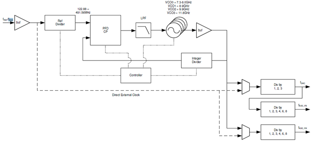
1. As our frequency range requirement is lower up to 100 MHz, so AFE7900EVM would be a suitable option. From the AFE7900 datasheet, I have found that there is an ADC sample rate divider (1,2,3,4,6 or 8), i.e. what I understand is that there is an internal ADC clock of 3 GSPS and then I have to use the division of 6 in order to provide 500 MSPS sampling rate to ADC, right?

2. In order to interface the AFE7900EVM to the Xilinx platform(ZCU102), TI-JESD204-IP is there, for which I have requested access. This IP core is free with the purchase of an evaluation board or there is any extra cost for the IP core?

3. The full-scale input power ADC range is given for different combinations of (Input frequency, ADC sample rate, NCO frequency, and Decimation selected). Is there any equation/calculation that needs to be done for defining the full-scale input power ADC range( let's say, Fin= 60 MHz, NCO freq=60 MHz, ADC sample rate=500 MSPS, decimation=16) what will be the full-scale input power ADC range?

4. I assume that the given full-scale input power range is single-ended and baluns are there in evaluation board, right?

5. My dynamic input range is 10mVP-P to 1Vp-p (-36 dBm to 4 dBm), so, I think, I need to use external VGA/DSA to be fall into the ADC input full scale power range? right?

6. With AFE7900EVM and ZCU102 evaluation board procurement, all other supporting resources are freely available or is there any extra cost for any of the resources?

Request for your quick support and guidance to further select the AFE7900EVM.

  • Hello support Team,

    Awaited your response on the above case.

  • Hi Maitry,

    1) On the AFE the ADCs have a lower limit of 1500MHz on the sampling rate, so you will not be able to directly sample at 500MSPS. However, with the 1500MHz or 3000MHz sampling rate you can use the DDC to achieve the 500MSPS data rate.

    2) The IP is provided royalty free with the use of TI converters.

    3) The full scale input power range for the ADC are given in the datasheet. These values are most dependent on the input frequency, as shown by the data points given in the datasheet. The NCO and decimation will not affect the full scale range and the sampling rates will have a very minimal effect on the full scale range.

    4) The given full-scale values in the datasheet are for a differential signal at the device pins.

    5) Yes, you can use an external VGA/DSA to fall into the ADC input full scale power range. One thing that could be helpful is that the RX chain also includes a programmable DSA.

    6) The supporting resources are freely available. 

    Regards,

    David Chaparro 

  • Hello support team,

    Thank you for your accurate guidance. For one thing , I still have a confusion regarding the ADC sample rate. 

    As per your saying for the ADC sample rate lower limit is 1500 MSPS , that means we need to use Fadc divider in such a way that Fadc = 1500 MSPS , right?

    Before I thought that we can use Fadc divider to provide direct 500 MSPS sample rate to ADC, but I think that is not correct.

    What I understand from your reply is that ADC (inside AFE79xx )'s minimum sample rate is 1500 MSPS. but then there are Rx decimation rates upto 48X , so we can decimate to the lowest possible sample rate in DDC using decimation factors.

    Actually our basic requirement is to use ADC with min 500 MSPS sample rate and final output rate requirement is 1 MSPS after decimation. But as AFE79XX ADC lower limit is 1500 MSPS , we can do below.

    ADC sample rate = 1500 MSPS , DDC decimation rate selection = highest ( 48X) = DDC output rate = 31.25 MSPS , and then further decimation upto 1 MSPS, we would need to do in the FPGA. 

    Please let me know if my understanding is correct and we can do as per above or there is any misunderstanding over here?

    Awaited your guidance and support.

  • Hi Maitry,

    You are correct, the minimum sample rate is 1500MSPS and you can use the decimation factor of 48 to achieve the output rate of 31.25 MSPS. If a lower data rate is required you can use the FGPA to decimate further.

    Regards,

    David Chaparro

  • Hello,

    Thank you for the response.