


Hello support team,
I have below queries related to internal AGC configuration.
1) I have gone through the schematic and realize that LNABypass pins(RXA, RXB, RXC, RXD ) are interfaced with the CPLD in AFE7900EVM board. and no pin is coming on the output header of AFE7900EVM board
In order to control the external LNA bypass/enable for all 4 channels, there is a requirement for use of Header pins through which I can provide voltage to control to external LNA.
So, As the RXA/RXB/RXC/RXD Bypass output signals are interfaced to CPLD only. Do I need to use CPLD as a buffer to transfer all 4 RXA, RXB, RXC, RXD Bypass output signals to FPGA through FMC connector and then FPGA Header pins to be used to interface external LNA? In short , The interfacing of RXBypass output signals needs to be interface with external LNA , how to interface that when that output signals are not coming to nay header directly?
2) If possible, do you have any application note that can describe internal AGC mechanism with external LNA control ? then it would be very helpful.
3) As given in the config guide, using internal AGC mechanism, either the complete LNA gain or part of the gain can be bypassed, So, I can choose the LNA in which gain can be controlled using voltage level.
My input range is very dynamic from minimum to maximum. so I have to use one fixed low gain LNA with another LNA (having variable gain , as It is not possible to choose fix gain LNA with bypass/enable)
(Example : Input amplitude Fixed gain LNA variable gain LNA ADC input
-40 dBm 12 dB 30 dB 2 dBm
-18 dBm 12 dB 12 dB 6 dBm
4 dBm 12 dB bypass 16 dBm
As you can see above , it is not possible to use only LNA with the functionality of bypass and enable as my input range variation is lower as well higher( -40 dBm to 5 dBm)
I need to use the LNA in which part of the gain can be bypass , full gain bypass, full gain enable as per requirement. For that, available VGA is 2 types 1) Voltage control VGA ( in which using 1 pin voltage variation, gain can be controlled) 2) DVGA
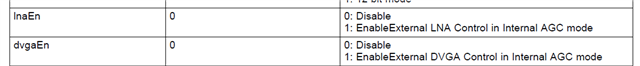
What I found from the configuration guide is as below screenshot, that in internal AGC mode, it is possible to control external DVGA . But I did not understand how to control external DVGA using single BYPASS control GPIO pin?
So using internal AGC mode is it possible to control the external VGA gain (so that part of the gain can be bypassed whenever required) Or it just capable to full bypass or full enable the external LNA?
4) Also, I found from the configuration guide that , ALC (Digital gain compensation) along with the internal AGC compensate the gain equivalent to current DSA attenuation as well External LNA current gain and phase by using lnagain0 and lnaphase0. So, I think, there is no need to read back the current DSA value and external LNA status through GPIO pin or SPI , as it is being compensated using DGC mechanism, Right? Please suggest if my understanding is correct?
I think, the main confusion over here for me with this internal AGC mechanism is the external Amplifier control (the amplifier , which should be having variable gain with bypass/enable, not the fixed gain with bypass/enable) . I request you to please provide guidance on the above list of queries as soon as possible so that I can finalize external amplifier for my application.
Awaited your quick response.
