Part Number: AFE7950EVM
Can AFE7950EVM run on Xilinx ZC706?
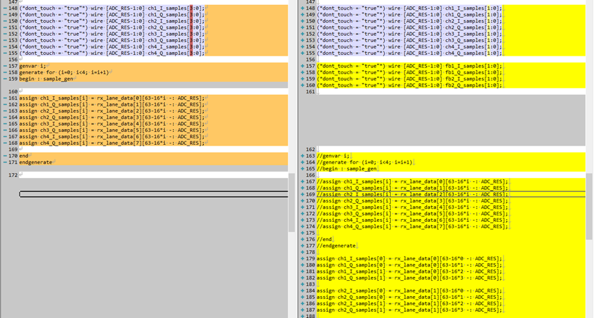
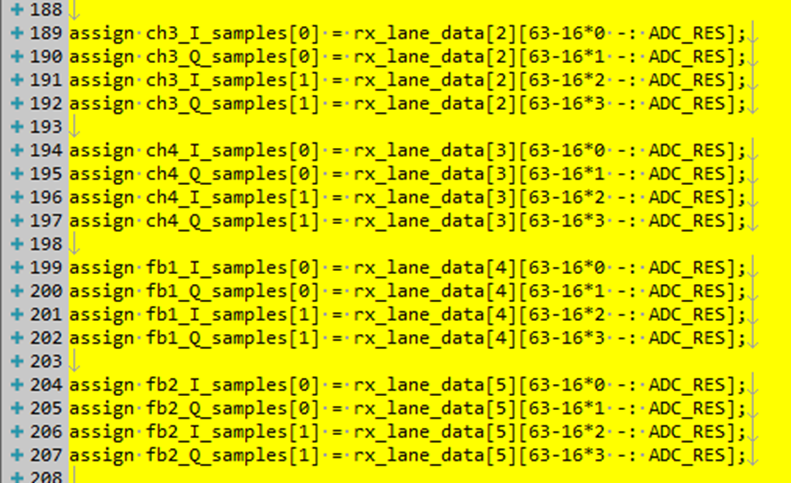
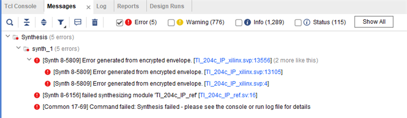
I want to develop program with LabVIEW and VIVADO. And I have get the TI-JESD204-IP but don't know how to start.
Can TI provide libraries and usages?
Original question:

Part Number: AFE7950EVM
Can AFE7950EVM run on Xilinx ZC706?
I want to develop program with LabVIEW and VIVADO. And I have get the TI-JESD204-IP but don't know how to start.
Can TI provide libraries and usages?