Hello,
The configuration I am using is as follows:
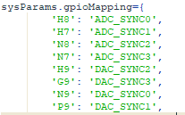
LMFSHdTx[14810] and LMFSHdRx [181610]
SYNC_IN connect LVDS and H8 and H7 pins. (SYNC_IN0)
SYNC_IN1 (N8 and N7) pins not connected.
SYNC_OUT connect LVDS and N9 and P9 pins. (SYNC_OUT1)
SYNC_OUT0 (H9 and G9) pins not connected.
GPIO Pins connect GPIO1….GPIO6.
But, I couldn't get the sync signals to work. The latte bring up file is as follows:
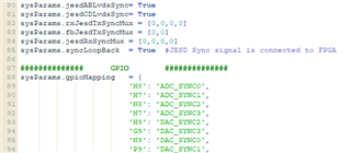
## The following parameters sets up the SYNCIN and SYNCOUT to interface with the TSW14J57
sysParams.jesdABLvdsSync = 1
sysParams.jesdCDLvdsSync = 1
sysParams.rxJesdTxSyncMux = [0,0,0,0]
sysParams.fbJesdTxSyncMux = [0,0]
sysParams.jesdRxSyncMux = [0,0,0,0] #[0,0,1,1]
sysParams.syncLoopBack = True
How should I set this place so that the sync signals work from the pins I specified?
Thank you,