
- Ask a related questionWhat is a related question?A related question is a question created from another question. When the related question is created, it will be automatically linked to the original question.
Original question:

Hi,
We are using AFE7769 in our design as per out layout requirements we are Planning to place SSRF section in the following manner..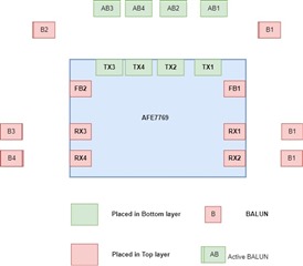
We are Planning to give isolation with shield on TOP and Bottom i.e (for TX & RX )
And ORX signal we are Planning to route in the internal layers with GND Planes on the top and Bottom.
For the feasibility of routing we might need to use one Via on single ended Signal for TX and RX


