


## sigSource2.frequency = 5.0e9
## sigSource2.amplitude = 10
## sigSource2.on = True
## LmkClkSrc.frequency = 1.0e9
## LmkClkSrc.amplitude = 10
## LmkClkSrc.on = True

sysParams=AFE.systemParams
sysParams.__init__();sysParams.chipVersion=chipVersion

setupParams.skipFpga 				= 1
sysParams							= AFE.systemParams
setupParams.fpgaRefClk 				= 250
AFE.systemStatus.loadTrims			= 1
sysParams.FRef                    	= 5000
sysParams.FadcRx                  	= 2500
sysParams.FadcFb				  	= 2500
sysParams.Fdac                    	= 2500*2
sysParams.rxEnable                  = [True]*4
sysParams.txEnable                  = [True]*4
sysParams.fbEnable                  = [False]*2
sysParams.externalClockTx			= True
sysParams.externalClockRx			= True

sysParams.enableDacInterleavedMode	= False 					#DAC interleave mode to save power consumption. Fs/2 - Fin spur occurs

sysParams.modeTdd 					= 0
										# 0- Single TDD Pin for all Channels
										# 1- Separate Control for 2T/2R/1F
										# 2- Separate Control for 1T/1R/1F

sysParams.RRFMode 					= 0   #4T4R2F FDD mode
sysParams.jesdSystemMode			= [1,1]
										#SystemMode 0:	2R1F-FDD						; rx1-rx2-fb-fb
										#SystemMode 1:	1R1F-FDD						; rx1-rx1-fb-fb
										#SystemMode 2:	2R-FDD							; rx1-rx1-rx2-rx2
										#SystemMode 3:	1R								; rx1-rx1-rx1-rx1
										#SystemMode 4:	1F								; fb-fb-fb-fb
										#SystemMode 5:	1R1F-TDD						; rx1/fb-rx1/fb-rx1/fb-rx1/fb
										#SystemMode 8:	1R1F-TDD 1R-FDD	(FB-2Lanes)(RX1 RX2 interchanged)		; rx2/fb-rx2/fb-rx1-rx1


sysParams.jesdLoopbackEn			= 0 #Make it 1 to Enable the JESDTX to JESDRX internal loopback
sysParams.LMFSHdRx                	= ['181610']*4
										# The 2nd and 4th are valid only for jesdSystemMode values in (2,6,7,8). For other modes, select 4 converter modes for 1st and 3rd.
sysParams.LMFSHdFb                	= ['24410']*4
sysParams.LMFSHdTx                	= ['14810']*4
sysParams.jesdTxProtocol            = [0,0]
sysParams.jesdRxProtocol            = [0,0]
sysParams.serdesFirmware			= True 		# If you want to lead any firmware, please speify the path here. Otherwise it will not write any firmware
#sysParams.jesdTxLaneMux				= [0,1,2,3,4,5,6,7]  #orj
sysParams.jesdTxLaneMux				= [0,1,2,3,4,5,6,7]		#OUR CONFIGURATION STx1 and SRx5 & SRx6
												# Enter which lanes you want in each location.
												# Note that across 2T Mux is not possible in 0.5.
												# For example, if you want to exchange the first two lines of each 2T, this should be [[1,0,2,3],[5,4,6,7]]
#sysParams.jesdRxLaneMux				= [0,4,2,3,1,5,6,7]	#orj
sysParams.jesdRxLaneMux				= [4,1,2,3,5,0,6,7]	#OUR CONFIGURATION STx1 and SRx5 & SRx6
												# Enter which lanes you want in each location.
												# Note that across 2R Mux is not possible in 0.5.
												# For example, if you want to exchange the first two lines of each 2R, this should be [[1,0,2,3],[5,4,6,7]]

sysParams.jesdRxRbd					= [3, 3]

sysParams.rxJesdTxScr				= [True,True,True,True]
sysParams.fbJesdTxScr				= [True,True]
sysParams.jesdRxScr					= [True,True,True,True]

sysParams.rxJesdTxK					= [4]*4
sysParams.fbJesdTxK					= [4]*2
sysParams.jesdRxK					= [4]*4

sysParams.ncoFreqMode 				= "FCW"

sysParams.txNco0					= 	[[3100,2800],		#Band0, Band1 for TxA for NCO0
										[3100,2800],        #Band0, Band1 for TxB for NCO0
										[3100,2800],        #Band0, Band1 for TxC for NCO0
										[3100,2800]]        #Band0, Band1 for TxD for NCO0

sysParams.rxNco0					= 	[[3100,2800],		#Band0, Band1 for RxA for NCO0
										[3100,2800],        #Band0, Band1 for RxB for NCO0
										[3100,2800],        #Band0, Band1 for RxC for NCO0
										[3100,2800]]        #Band0, Band1 for RxD for NCO0

sysParams.fbNco0					= 	[3100,2800]			#FBA, FBC for NCO0
sysParams.fbNco1					= 	[3100,2800]			#FBA, FBC for NCO1
sysParams.fbNco2					= 	[3100,2800]			#FBA, FBC for NCO2
sysParams.fbNco3					= 	[3100,2800]			#FBA, FBC for NCO3

sysParams.numBandsRx				= [0]*4					# 0 for single, 1 for dual
sysParams.numBandsFb				= [0,0]
sysParams.numBandsTx				= [0,0,0,0]

sysParams.ddcFactorRx             	= [40]*4			# DDC decimation factor for RX A, B, C and D
sysParams.ddcFactorFb             	= [10]*2
sysParams.ducFactorTx             	= [40]*4

## The following parameters sets up the LMK04828 clocking schemes
lmkParams.pllEn						=	False#True#
lmkParams.inputClk					=	1000#1000 di
lmkParams.sysrefFreq				=	2500./768
lmkParams.lmkFrefClk				=	False

## The following parameters sets up the register and macro dumps
logDumpInst.setFileName(ASTERIX_DIR+DEVICES_DIR+r"\Afe79xxPg1.txt")
logDumpInst.logFormat				= 0x01
logDumpInst.rewriteFile				= 1
logDumpInst.rewriteFileFormat4		= 1
device.optimizeWrites				= 0
device.rawWriteLogEn				= 1

## The following parameters sets up the SYNCIN and SYNCOUT to interface with the TSW14J57
sysParams.jesdABLvdsSync			= 1
sysParams.jesdCDLvdsSync			= 1
sysParams.rxJesdTxSyncMux			= [0,0,0,0]
sysParams.fbJesdTxSyncMux			= [0,0]
sysParams.jesdRxSyncMux				= [0,0,0,0]		#[0,0,1,1]
sysParams.syncLoopBack				= True

# ## The following parameters sets up the AGC
# sysParams.agcParams[0].agcMode = 1 ##internal AGC
# sysParams.agcParams[0].gpioRstEnable = 0 ##disable GPIO based reset to AGC detector
# sysParams.agcParams[0].atken = [0, 1, 0] ##enable big and small step attack
# sysParams.agcParams[0].decayen = [0,1,0] ##enable big and small step decay
# sysParams.agcParams[0].atksize = [2,1,0] ## bigs step = 2dB, small step = 1dB
# sysParams.agcParams[0].decaysize = [2,1,0] ##big step = 2dB, small step = 1dB
# sysParams.agcParams[0].atkthreshold = [-1, -2, -14] ##attack threshold
# sysParams.agcParams[0].decaythreshold = [-14, -6, -20] ##decay threshold
# sysParams.agcParams[0].atkwinlength = [170, 170] ## detector time constant expressed inn absolute time in ns.
# sysParams.agcParams[0].decaywinlength = 87380 ##detector time constant expressed in absolute time in ns. All detectors use the same value for decay time constant
# sysParams.agcParams[0].atkNumHitsAbs = [8,8] ##absolute number of times signal crosses threshold. These crossing are with respect to the FADC/8 clock
# sysParams.agcParams[0].decayNumHitsAbs = [100,100] ##absolute number of times signal crosses threshold. These crossing are with respect to the FADC/8 clock
# sysParams.agcParams[0].minDsaAttn = 0 ##minimum DSA attenuation used by AGC
# sysParams.agcParams[0].maxDsaAttn = 22 ##maximum DSA attenuation used by AGC
# sysParams.agcParams[0].totalGainRange = 22 ##total gain range used by ALC for gain compensation
# sysParams.agcParams[0].minAttnAlc = 0 ##minimum attenuation used by ALC for compensation when useMinAttnAgc = 0
# sysParams.agcParams[0].useMinAttnAgc = 1 ##enable ALC to use minimum attenuation from AGC for which compensation is required.
# sysParams.agcParams[0].alcEn = 1
# sysParams.agcParams[0].alcMode = 0 ##floating point DGC
# sysParams.agcParams[0].fltPtMode = 0 ##if exponent > 0, dont send MSB
# sysParams.agcParams[0].fltPtFmt = 1 ##3 bit exponent


## The following parameters sets up the GPIOs
sysParams.gpioMapping={
		'H8': 'ADC_SYNC0',
		'H7': 'ADC_SYNC1',
		'N8': 'ADC_SYNC2',
		'N7': 'ADC_SYNC3',
		'H9': 'DAC_SYNC2',
		'G9': 'DAC_SYNC3',
		'N9': 'DAC_SYNC0',
		'P9': 'DAC_SYNC1',
		'P14': 'GLOBAL_PDN',
		'K14': 'FBABTDD',
		'R6': 'FBCDTDD',
		'H15': ['TXATDD','TXBTDD'],
		'V5': ['TXCTDD','TXDTDD'],
		'E7': ['RXATDD','RXBTDD'],
		'R15': ['RXCTDD','RXDTDD']}

#AFE.systemParams.papParams[0]['enable'] = True
#AFE.systemParams.papParams[1]['enable'] = True
#AFE.systemParams.papParams[2]['enable'] = True
#AFE.systemParams.papParams[3]['enable'] = True

device.delay_time = 0
## Initiates LMK04828 and AFE79xx Bring-up
AFE.deviceBringup()

AFE.TOP.overrideTdd(15,3,15)
Design Overview
The system has 2-link 10 Gbps lane rate and LMFS=14810 lane configuration with communicate the AFE7900. For this specs, FPGA design has two Xilinx RX JESD204 IP, two Xilinx TX JESD204 IP and two JESD204 PHY for 16 AFE. Figure 1 shows that the FPGA-AFE connection in the design. The SYSREF is created by FPGA which has same clock domain with AFE REFCLK.

Figure 1 - AFE-FPGA Connection Scheme
Questions
1) We are working on the FPGA with the configuration set created with the Latte Python script and the design we mentioned above. During our tests, we don’t have stable link. Sometimes we can see the sync_in and sync_out signals of some AFEs as HIGH, however we can’t see most of time. We have some SPI errors as described below. What is the meaning of these errors ? What we can do the debug and fix these errors ?
We have 7 Errors. 1 of them from ADC JESD Register Page and the others from DAC JESD Register Page (3 from DAC AB Page and 3 from DAC CD Page)
ADC JESD Register Map
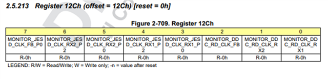
- Register 12Ch expected is 0x08 but have 0xF7. What is the meaning of this register and why could we have this error ?
DAC JESD Register Map (Both AB and CD Pages)
We have 3+3 errors at this page as belows. Why could we have these errors and what can we do the fix these errors ?
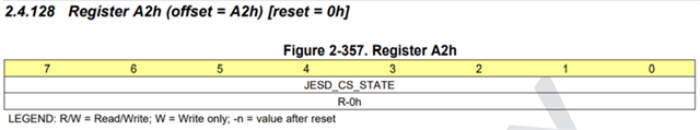
- Register A2h, expected value is 0x02 but we have 0x00.
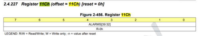
- Register 11Ch, expected value is 0x00 and we have 0x00 but we got error at this address. We don’t know why but the reason can be timeout.
- Register EEh, expected value is 0x01 but we have 0x00.

2) We asked the below question to TI and they replied as below. We tried to test DACs with Constant test pattern (Using B7h in DAC JESD Page). But we have seen that only AFEs that could be sync can outputs the signal. Since, we don’t have a stable link we could not perform a proper test in this way. Do AFEs need to be sync to perform this test? Our test pattern is shared below.
Test Pattern:
Register 18 -> 00
Register 15 -> 00
Register 16 -> 04
Register B7 -> 01
Register 16 -> 08
Register B7 -> 01
Our Question and TI reply is shared below.
Q: We suspects the clock source of board so we want to check this. Our board has 5 GHz clock source (A signal Generator). We check this clock with Spectrum Analyzer and it seems that the clock source is ok. But, when I read Register 0x15F on the JESD_SUBCHIP page, AFE returns 0x03. The register indicating SerdesAB and SerdesCD PLL loss-of-lock. How should we make sense of this? Is there any SPI register and/or command set to decide whether the clock source is okay or not?
DC: When using an external clock we do not have a register that can be read to check if the clock is present. One thing that can be done is to program the AFE DAC channels into the constant output Test Pattern mode. This mode will make it so that the DACs output only the NCO frequency regardless of the data they are receiving. If the DAC output looks good in this mode then we can verify that the AFE is receiving the external clock. To put the AFE into this mode you can run the following lines in Latte:
