This thread has been locked.

If you have a related question, please click the "Ask a related question" button in the top right corner. The newly created question will be automatically linked to this question.

AFE7950EVM: AFE7950EVM_TSW14J56 Interface

Part Number: AFE7950EVM


Hi,

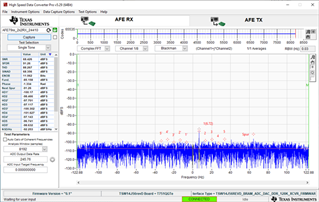
Currently I am using AFE7950EVM with TSW14J56 capture card to evaluate the ADC. I have followed the steps mentioned in user guide for HSDC pro and Latte script. In the log window it is showing that link is established between both the boards (also confirmed from the status LED D2 and D4 blinking). But while sending the tone from HSDC pro DAC tab and capturing the same from ADC tab nothing appears. In addition to this I am unable to observe this tone on spectrum analyzer.

ADC Captured data

Why this much of low output level?

  • Hi Akash,

    Can you confirm that the input tone to the Rx inputs is close the NCO frequency set in the Latte script, usually for testing purposes I set the the signal generator to the NCO+20MHz? For the default scripts then the RxA channel has the NCO set to 5.4GHz so you can send a 5.42GHz signal and capture the tone in HSDC Pro.  If you are using the default scripts then what you can do to test is loopback the TxA output to the RxA input and capture the DAC tone. 

    Also, in HSDC Pro for the Rx channel you should set the window to Complex FFT.

    Regards,

    David Chaparro

  • Thanks David for your prompt reply.

    As per the below image there are two frequency set for NCO i.e. 3500 and 2600. Why this two band mentioned in the code? And what is the reason for giving

    input signal with frequency close to NCO frequency?

  • Hi Akash,

    The reason that you can program two values into the NCO, 3500 and 2600, is for when you program the Tx or Rx to operate in Dual Band mode. In this mode there will be two DUCs or DDCs per channel and the NCO can be set for both of the DUCs/DDCs. The script that you are showing is set for single band mode so the second value, 2600, is not used and your NCOs are set to 3.5GHz. Please see section 8.3.3 for more information on this for the Tx side. 

    The reason that I say the input frequency should be close to the NCO frequency is because for the configuration you are showing the Rx is configured for a IBW of 245.76MHz, so with the NCO set to 3.5GHz the input frequency should be within 3.5GHz +- 122.88MHz. For testing purposes I usually set the input frequency to NCO + 20MHz. 

    Regards,

    David Chaparro 

  • Hi David,

    Thank you for your response.

    Could you share any design example or application note in which device used in dual band mode?

    Regards,

    Akash Gupta

  • Hi Akash,

    The script below can be used as a reference with for dual band mode. Please note that in HSDC Pro you should select the Dual Band ini file, 28810.

    ##############		Read me			##############
    #In HSDC Pro DAC tab, Select AFE79xx_2x2TX_44210; Data Rate = 491.52M
    #In HSDC Pro ADC tab, Select AFE79xx_2x2RX_44210; Data Rate = 491.52M ---> To capture 4 RX channels
    
    sysParams=AFE.systemParams
    sysParams.__init__();sysParams.chipVersion=chipVersion
    
    setupParams.skipFpga = 1 # setup FPGA (TSW14J56) using HSDC Pro 
    ##############		Top Level			##############
    sysParams.FRef			= 491.52
    sysParams.FadcRx		= 2949.12
    sysParams.FadcFb		= 2949.12
    sysParams.Fdac			= 2949.12*4
    sysParams.externalClockRx=False
    sysParams.externalClockTx=False
    													
    ##############		Digital Chain		##############
    
    		#####	RX	#####
    sysParams.ddcFactorRx	=	[24,24,24,24]				#DDC decimation factor for RX A, B, C and D
    sysParams.rxNco0		= 	[[9500,9520],			#Band0, Band1 for RXA 
    							[9500,9520],        	#Band0, Band1 for RXB 
    							[9500,9520],        	#Band0, Band1 for RXC 
    							[9500,9520]]        	#Band0, Band1 for RXD 
    sysParams.numBandsRx	=	[1]*4         			# 0 for single, 1 for dual
    
    		#####	FB	#####
    sysParams.fbEnable		=	[False,False]
    sysParams.ddcFactorFb	=	[6,6]					#DDC decimation factor for FB 1 and 2
    sysParams.fbNco0		= 	[9500,9500]				#Band0 for FB1 and FB2 
    
    		#####	TX	#####
    sysParams.ducFactorTx	=	[96,96,96,96]			#DUC interpolation factor for TX A, B, C and D
    sysParams.txNco0		= 	[[9500,9520],			#Band0, Band1 for TXA 
    							[9500,9520],        	#Band0, Band1 for TXB 
    							[9500,9520],        	#Band0, Band1 for TXC 
    							[9500,9520]]        	#Band0, Band1 for TXD
    sysParams.numBandsTx	= 	[1]*4					# 0 for single, 1 for dual
    
    ##############		JESD		##############
    
    		#####	ADC-JESD	#####
    sysParams.jesdSystemMode= [3,3]
    													#SystemMode 0:	2R1F-FDD						; rx1-rx2-fb -fb
    													#SystemMode 1:	1R1F-FDD						; rx -rx -fb -fb
    													#SystemMode 2:	2R-FDD							; rx1-rx1-rx2-rx2
    													#SystemMode 3:	1R								; rx -rx -rx -rx
    													#SystemMode 4:	1F								; fb -fb- fb -fb
    													#SystemMode 5:	1R1F-TDD						; rx/fb-rx/fb-rx/fb-rx/fb
    													
    sysParams.jesdTxProtocol= [0,0]						# 0 - 8b/10b encoding; 2 - 64b/66b encoding 
    sysParams.LMFSHdRx		= ["28810","28810","28810","28810"]
    													# The 2nd and 4th are valid only for jesdSystemMode values in (0,2).
    													# For other modes, select 4 converter modes for 1st and 3rd.
    sysParams.LMFSHdFb		= ["22210","22210"]
    
    sysParams.rxJesdTxScr	= [True,True,True,True]
    sysParams.fbJesdTxScr	= [True,True]
    
    sysParams.rxJesdTxK		= [16,16,16,16]
    sysParams.fbJesdTxK		= [16,16]
    
    sysParams.jesdTxLaneMux	= [0,1,2,3,4,5,6,7]			# Enter which lanes you want in each location. 
    													# For example, if you want to exchange the first two lines of each 2T,
    													#		this should be [[1,0,2,3],[5,4,6,7]]
    
    		#####	DAC-JESD	#####
    sysParams.jesdRxProtocol= [0,0]
    sysParams.LMFSHdTx		= ["28810","28810","28810","28810"]
    sysParams.jesdRxLaneMux	= [0,1,2,3,4,5,6,7]			# Enter which lanes you want in each location.
    													# For example, if you want to exchange the first two lines of each 2R
    													#		this should be [[1,0,2,3],[5,4,6,7]]
    sysParams.jesdRxRbd		= [4, 4]
    sysParams.jesdRxScr		= [True,True,True,True]
    sysParams.jesdRxK		= [16,16,16,16]
    
    		#####	JESD Common	#####
    	
    sysParams.jesdABLvdsSync= True
    sysParams.jesdCDLvdsSync= True
    sysParams.syncLoopBack	= True	#JESD Sync signal is connected to FPGA
    
    ##############		GPIO		##############
    sysParams.gpioMapping	= {
    						'H8': 'ADC_SYNC0',
    						'H7': 'ADC_SYNC1',
    						'N8': 'ADC_SYNC2',
    						'N7': 'ADC_SYNC3',
    						'H9': 'DAC_SYNC0',
    						'G9': 'DAC_SYNC1',
    						'N9': 'DAC_SYNC2',
    						'P9': 'DAC_SYNC3',
    						'P14': 'GLOBAL_PDN',
    						'K14': 'FBABTDD',
    						'R6': 'FBCDTDD',
    						'H15': ['TXATDD','TXBTDD'],
    						'V5': ['TXCTDD','TXDTDD'],
    						'E7': ['RXATDD','RXBTDD'],
    						'R15': ['RXCTDD','RXDTDD']}
    
    ##############		LMK Params		##############
    lmkParams.pllEn			= True
    lmkParams.inputClk		= 983.04 # Valid only when lmkParams.pllEn = False
    lmkParams.lmkFrefClk	= True
    setupParams.fpgaRefClk	= 245.76 # Should be equal to LaneRate/40 for TSW14J56
    
    ##############		Logging		##############
    logDumpInst.setFileName(ASTERIX_DIR+DEVICES_DIR+r"\Afe79xxPg1.txt")
    logDumpInst.logFormat=0x0 #Modify to 0x1 to save register scequence to log file. Script takes more time to execute.
    logDumpInst.rewriteFile=1
    logDumpInst.rewriteFileFormat4=1
    device.optimizeWrites=0
    device.rawWriteLogEn=1
    
    device.delay_time = 0
    #-------------------------------------------------------------------------------------------------#
    AFE.deviceBringup()
    
    AFE.TOP.overrideTdd(15,3,15)	# bit-wise; 4R,2F,4T

    Regards,

    David Chaparro

  • Hi David,

    Thanks for your reply.