This thread has been locked.

If you have a related question, please click the "Ask a related question" button in the top right corner. The newly created question will be automatically linked to this question.

AFE7950EVM: Clocking diagram from external clock reference

Part Number: AFE7950EVM
Other Parts Discussed in Thread: AFE7950, LMK04832

Hi Team,

I wanted to check with you how is the external clock (e.g. 163.68 MHz) provided to the AFE7950EVM on connector J14 distributed throughout the evaluation board.

I understand that AFE7950 system clock lane will be necessary (from which e.g. ADC and DAC sampling rates will be derived), but also there is the LMK that sends multiple outputs, some of which are going towards the FPGA (in this setup FPGA is connected to the AFE eval. module).

Does the LMK take as input the external clock and then provide all the necessary clock outputs to both AFE and FPGA, or is there any additional clock signal splitting happening on the eval board?

In addition, is the same clocking distribution then applied to the AFE7950 device in standalone mode (without eval board that comes with extra LMK and other components), given that the user provides dedicated LMK device?

Kind regards,

Željko

  • Hi Željko,

    We need one or two more days to look into this and respond. I apologize for the delay. 

    Regards,

    Vijay

  • Hi Zeljko,

    On our the EVM we provide the LMK with an external 163.68MHz signal and bypass this signal to the AFE. For the FPGA clocks the LMK takes this input signal and divides it down by 2 as our FPGA was configured to expect a input of 81.84MHz.

    In this configuration the LMK provides clocks to both the AFE and FPGA. 


    Regards,

    David Chaparro

  • Hi David,

    Thanks for the reply.

    How many LMK outputs are being used by AFE and how many by the FPGA?

    I ask this because in our current setup there is an external reference clock (163.68 MHz) brought to both AFE (J14) and the FPGA. FPGA uses this main clock as a system clock. If I understand correctly from what you said and also based on the AFE EVM schematics, from J14 signal goes to the LMK, and from LMK there are 2 clock signals going to the AFE chip, and 1 signal to the FPGA (for the JESD transceivers).

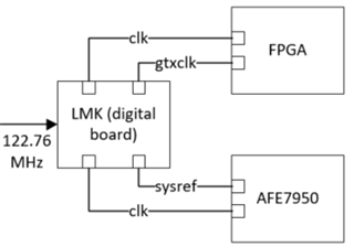
    For the flight version of this project we are looking into very similar setup, but I am considering using an LMK (e.g. LMK04832) that would be generating all of the clocks at the same place for both the FPGA and AFE7950. Practically, this would mean that now the LMK comes before J14 and it sends directly all the necessary clocks to the AFE and FPGA. For this I provided a simplified clocking block diagram below. Note that in this setup the clock is a bit lower that it is in the current considerations (122.76MHz=10.23x12, instead of 163.68MHz=10.23x16) so we can achieve higher JESD204b lane-rates (9820.8 Mb/s=122.76x80).

    Kind regards,

    Željko

  • Hi Zeljko,

    Two LMK outputs are used by the AFE, one for the AFE refclk and one for the SYSREF. On the FPGA side the LMK is providing three outputs, one for SYSREF and two clocks, JESD coreclock and transceiver clock. More information on the clocking for the FPGA and TI IP are given in the TI204c-IP-Users-Guide, section 6.4. 

    Regards,

    David Chaparro

  • Hi David,

    Much appreciate your response and the information therein.

    One final thing, after which we can close this thread from my side.

    Is this what you say above (3 clock outputs to the FPGA) a general approach/information valid for any kind of FPGA (in particular Xilinx XQRKU060), or is it related only to the reference design you provided me recently?

    Kind regards,

    Željko

  • Hi Zeljko,

    If using the TI JESD IP 3 clocks, 2 clocks and 1 SYSREF, are required. Please see the TI204c IP user's guide clocking section for additional information. Other IPs may only require 2 clocks, 1 clock and 1 SYSREF, but I would recommend reading up on their documentation before deciding. 

    Regards,

    David Chaparro