Part Number: AFE7900EVM
Other Parts Discussed in Thread: LMK04828
Hi Experts:
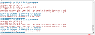
I encountered DAC JESD-Rx link errors while running FPGA and AFE7900EVM.
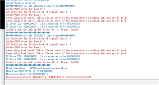
The K value is also set to 32 on the FPGA end,
Is there something wrong with my Settings?
I used 1 link 48810 mode with an IP core on the FPGA side.
In my understanding, sync setting the same value can be treated as the same link on the FPGA side,
Am I getting this right?
setupParams.skipFpga 				= 1
sysParams							=	AFE.systemParams
setupParams.fpgaRefClk 				= 245.76
AFE.systemStatus.loadTrims			= 1

sysParams.FRef                    	= 491.52
sysParams.FadcRx                  	= 2949.12
sysParams.FadcFb				  	= 2949.12
sysParams.Fdac                    	= 2949.12*3
sysParams.rxEnable                  =[False,False,False,False]

sysParams.enableDacInterleavedMode	= False 					#DAC interleave mode to save power consumption. Fs/2 - Fin spur occurs

sysParams.modeTdd 					= 0
										# 0- Single TDD Pin for all Channels
										# 1- Separate Control for 2T/2R/1F
										# 2- Separate Control for 1T/1R/1F

sysParams.topLevelSystemMode		= 'StaticTDDMode'
sysParams.RRFMode 					= 0   #4T4R2F FDD mode
sysParams.jesdSystemMode			= [1,1]
										#SystemMode 0:	2R1F-FDD						; rx1-rx2-fb-fb
										#SystemMode 1:	1R1F-FDD						; rx1-rx1-fb-fb
										#SystemMode 2:	2R-FDD							; rx1-rx1-rx2-rx2
										#SystemMode 3:	1R								; rx1-rx1-rx1-rx1
										#SystemMode 4:	1F								; fb-fb-fb-fb
										#SystemMode 5:	1R1F-TDD						; rx1/fb-rx1/fb-rx1/fb-rx1/fb
										#SystemMode 8:	1R1F-TDD 1R-FDD	(FB-2Lanes)(RX1 RX2 interchanged)		; rx2/fb-rx2/fb-rx1-rx1


sysParams.jesdLoopbackEn			= 0 #Make it 1 to Enable the JESDTX to JESDRX internal loopback
sysParams.LMFSHdRx                	=['24410', '24410', '24410', '24410']
										# The 2nd and 4th are valid only for jesdSystemMode values in (2,6,7,8). For other modes, select 4 converter modes for 1st and 3rd.
sysParams.LMFSHdFb                	= ["22210","22210"]
sysParams.LMFSHdTx                	= ["24410","24410","24410","24410"]
sysParams.jesdTxProtocol            = [0,0]
sysParams.jesdRxProtocol            = [0,0]
sysParams.serdesFirmware			= True 		# If you want to lead any firmware, please speify the path here. Otherwise it will not write any firmware
sysParams.jesdTxLaneMux				= [0,1,2,3,4,5,6,7]
												# Enter which lanes you want in each location.
												# Note that across 2T Mux is not possible in 0.5.
												# For example, if you want to exchange the first two lines of each 2T, this should be [[1,0,2,3],[5,4,6,7]]
sysParams.jesdRxLaneMux				= [0,1,2,3,4,5,6,7]
												# Enter which lanes you want in each location.
												# Note that across 2R Mux is not possible in 0.5.
												# For example, if you want to exchange the first two lines of each 2R, this should be [[1,0,2,3],[5,4,6,7]]

sysParams.jesdRxRbd					= [4, 4]

sysParams.rxJesdTxScr				= [False,False,False,False]
sysParams.fbJesdTxScr				= [False,False]
sysParams.jesdRxScr					= [False,False,False,False]

sysParams.rxJesdTxK					= [32,32,32,32]
sysParams.fbJesdTxK					= [32,32]
sysParams.jesdRxK					= [32,32,32,32]

sysParams.ncoFreqMode 				= "1KHz"

sysParams.txNco0					= 	[[200,200],		#Band0, Band1 for TxA for NCO0
										[200,200],        #Band0, Band1 for TxB for NCO0
										[200,200],        #Band0, Band1 for TxC for NCO0
										[200,200]]        #Band0, Band1 for TxD for NCO0

sysParams.rxNco0					= 	[[2600,2600],		#Band0, Band1 for RxA for NCO0
										[9500,2600],        #Band0, Band1 for RxB for NCO0
										[9500,2600],        #Band0, Band1 for RxC for NCO0
										[9500,2600]]        #Band0, Band1 for RxD for NCO0

sysParams.fbNco0					= 	[9500,9500]			#FBA, FBC for NCO0
sysParams.fbNco1					= 	[9500,9500]			#FBA, FBC for NCO1
sysParams.fbNco2					= 	[9500,9500]			#FBA, FBC for NCO2
sysParams.fbNco3					= 	[9500,9500]			#FBA, FBC for NCO3

sysParams.numBandsRx				= [0]*4					# 0 for single, 1 for dual
sysParams.numBandsFb				= [0,0]
sysParams.numBandsTx				= [0,0,0,0]

sysParams.ddcFactorRx             	= [12,12,12,12]			# DDC decimation factor for RX A, B, C and D
sysParams.ddcFactorFb             	= [6,6]
sysParams.ducFactorTx             	= [36,36,36,36]


## The following parameters sets up the LMK04828 clocking schemes
lmkParams.pllEn						=	True#False
lmkParams.inputClk					=	1474.56#737.28
lmkParams.sysrefFreq				=	3.84
lmkParams.lmkFrefClk				=	True

## The following parameters sets up the register and macro dumps
logDumpInst.setFileName(ASTERIX_DIR+DEVICES_DIR+r"\Afe79xxPg1.txt")
logDumpInst.logFormat				= 0x0f
logDumpInst.rewriteFile				= 1
logDumpInst.rewriteFileFormat4		= 1
device.optimizeWrites				= 0
device.rawWriteLogEn				= 1

## The following parameters sets up the SYNCIN and SYNCOUT to interface with the TSW14J57
sysParams.jesdABLvdsSync			= 1
sysParams.jesdCDLvdsSync			= 1
sysParams.rxJesdTxSyncMux			= [0,0,0,0]
sysParams.fbJesdTxSyncMux			= [0,0]
sysParams.jesdRxSyncMux				= [0,0,0,0]		#[0,0,1,1]
sysParams.syncLoopBack				= True

# ## The following parameters sets up the AGC
# sysParams.agcParams[0].agcMode = 1 ##internal AGC
# sysParams.agcParams[0].gpioRstEnable = 0 ##disable GPIO based reset to AGC detector
# sysParams.agcParams[0].atken = [0, 1, 0] ##enable big and small step attack
# sysParams.agcParams[0].decayen = [0,1,0] ##enable big and small step decay
# sysParams.agcParams[0].atksize = [2,1,0] ## bigs step = 2dB, small step = 1dB
# sysParams.agcParams[0].decaysize = [2,1,0] ##big step = 2dB, small step = 1dB
# sysParams.agcParams[0].atkthreshold = [-1, -2, -14] ##attack threshold
# sysParams.agcParams[0].decaythreshold = [-14, -6, -20] ##decay threshold
# sysParams.agcParams[0].atkwinlength = [170, 170] ## detector time constant expressed inn absolute time in ns.
# sysParams.agcParams[0].decaywinlength = 87380 ##detector time constant expressed in absolute time in ns. All detectors use the same value for decay time constant
# sysParams.agcParams[0].atkNumHitsAbs = [8,8] ##absolute number of times signal crosses threshold. These crossing are with respect to the FADC/8 clock
# sysParams.agcParams[0].decayNumHitsAbs = [100,100] ##absolute number of times signal crosses threshold. These crossing are with respect to the FADC/8 clock
# sysParams.agcParams[0].minDsaAttn = 0 ##minimum DSA attenuation used by AGC
# sysParams.agcParams[0].maxDsaAttn = 22 ##maximum DSA attenuation used by AGC
# sysParams.agcParams[0].totalGainRange = 22 ##total gain range used by ALC for gain compensation
# sysParams.agcParams[0].minAttnAlc = 0 ##minimum attenuation used by ALC for compensation when useMinAttnAgc = 0
# sysParams.agcParams[0].useMinAttnAgc = 1 ##enable ALC to use minimum attenuation from AGC for which compensation is required.
# sysParams.agcParams[0].alcEn = 1
# sysParams.agcParams[0].alcMode = 0 ##floating point DGC
# sysParams.agcParams[0].fltPtMode = 0 ##if exponent > 0, dont send MSB
# sysParams.agcParams[0].fltPtFmt = 1 ##3 bit exponent


## The following parameters sets up the GPIOs
sysParams.gpioMapping={
		'H8': 'ADC_SYNC0',
		'H7': 'ADC_SYNC1',
		'N8': 'ADC_SYNC2',
		'N7': 'ADC_SYNC3',
		'H9': 'DAC_SYNC0',
		'G9': 'DAC_SYNC1',
		'N9': 'DAC_SYNC2',
		'P9': 'DAC_SYNC3',
		'P14': 'GLOBAL_PDN',
		'K14': 'FBABTDD',
		'R6': 'FBCDTDD',
		'H15': ['TXATDD','TXBTDD'],
		'V5': ['TXCTDD','TXDTDD'],
		'E7': ['RXATDD','RXBTDD'],
		'R15': ['RXCTDD','RXDTDD']}

#AFE.systemParams.papParams[0]['enable'] = True
#AFE.systemParams.papParams[1]['enable'] = True
#AFE.systemParams.papParams[2]['enable'] = True
#AFE.systemParams.papParams[3]['enable'] = True


## Initiates LMK04828 and AFE79xx Bring-up
setupParams.skipLmk	=	False

AFE.initializeConfig()

lmkParams.sysrefFreq = AFE.systemStatus.sysrefFreq
lmkParams.lmkPulseSysrefMode = False
AFE.LMK.lmkConfig()
## Initiates AFE79xx Bring-up
setupParams.skipLmk	=	True
AFE.deviceBringup()

AFE.TOP.overrideTdd(15,3,15)
Good day