This thread has been locked.

If you have a related question, please click the "Ask a related question" button in the top right corner. The newly created question will be automatically linked to this question.

AFE7950: Is there a feature that allows alignment of NCO phase between internal channels?

Part Number: AFE7950
Other Parts Discussed in Thread: LMK04828,

Hello,

I am developing an mmWave application using two AFE7950 devices.
My board consists of an MPSoC (XCZU11EG@AMD) + LMK04828 + AFE7950(x2) configuration.

1. Is the AFE7950 device suitable for my mmWave application, including beamforming?

2. Is there a feature in the AFE7950 that allows alignment of NCO phase between internal channels?
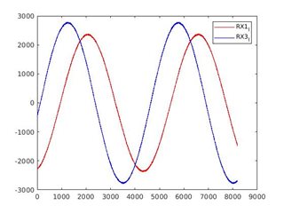
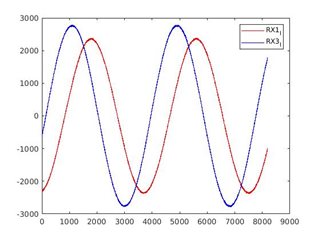
There seems to be a phase difference between TX/RX channels.
When powering on/off, the phase difference remains constant (e.g., Ch2-Ch1: 55°).
This appears to be due to the internal NCO phase difference in the AFE7950.
Is there a feature in the AFE7950 that allows alignment of NCO phase between internal channels?
Alternatively, should I correct this using the NCOx_PHASE_OFFSET register?

Thank you!

Regards,

Park.

  • Hi Park,

    Yes, the AFE7950 is suitable for mmWave applications, including beamforming. 

    Inside the AFE the phase of the NCOs are aligned. The difference that you are seeing is caused by the difference in the routing. On the AFE7950 substrate and the AFE7950EVM the routing for each of the channels is not the same, which is causing the constant phase difference that you are seeing. 

    If you would like to align the NCOs such that the phase difference is 0 the I would recommend using the NCOx_PHASE_OFFSET registers. 

    Regards,

    David Chaparro 

  • Hi David,

    Thank you for your response.

    Unfortunately, it seems that in my case, the phase alignment within the AFE7950 is not working as expected (attached Latte Log file).

    I input the CW signal into the RX channels through a splitter (1:2).
    1. NCO=4000MHz Fin=4000.1MHz


    => Phase difference between Channel 1 and Channel 3: -65.405˚ (-1816.8ns)
    2. NCO=4000MHz Fin=4000.12MHz


    => Phase difference between Channel 1 and Channel 3: -65.443˚ (-1514.9ns)

    If the NCO phases within the AFE7950 are aligned and the phase discrepancy is due to routing differences, there should not be a difference in absolute timing.

    In this case, it appears to be an issue with the lack of alignment in NCO phases between the channels.

    Could you provide information from the attached Latte Log file indicating the locations where the NCO phases are aligned?

    Please provide guidance on potential solutions to address this problem.

    Thank you.

    Regards,

    Park.

    2023.08.21_mmWave_AFE7950_R01.txt


  • I have an additional question.

    For the RX channels, I have confirmed that the phase can be changed using the RX_DDC_BAND0_NCO0_PHASE_OFFSET register.

    However, for the TX channels, even when I write values to the TX_DUC_BAND0_MIXER1_NCO0_PHASE_OFFSET register, the output phase does not change.

    Is there any additional action required to change the phase for the TX channels?

    Regards,

    Park.

  • I have some additional information that I would like to inquire about.

    1. AFE795EVM Board Test
    I have confirmed the occurrence of a phase difference between RX Ch1 and Ch2 during testing with the E/V Kit.
    Even after changing the frequency, the phase difference (Angle) remains the same.
    To align the phase difference between channels to zero on the E/V Kit, is it correct to use the NCOx_PHASE_OFFSET register?
       

    2. TX Channel NCO Phase Offet
    In the previous experiment, even when values were written to the TX_DUC_BAND0_MIXER1_NCO0_PHASE_OFFSET register, the output phase didn't change. 
    However, after changing the VCO (7372.8MHz -> 11796.48MHz(=DAC Sampling Clock)), I confirmed that the output phase did change. 
    Was there a specific reason why the output phase didn't change before the VCO was modified?

    Could you please provide an answer to my question.

    Regards,

    Park.

  • Hi Park,

    The NCOx_Phase_Offset register should be used to align the phase difference between channels to zero. It is expected to work for both Rx and Tx. I am working on testing on my bench to see why it did not work for the 7372.8MHz case. 

    Regards,

    David Chaparro

  • Hi Park,

    Can you share the script that you used for the 7372.8MSPS case? 

    I tested with the below script and faced no issue updating the Tx NCO phase.

    ##############		Read me			##############
    #In HSDC Pro DAC tab, Select AFE79xx_2x2TX_44210; Data Rate = 491.52M
    #In HSDC Pro ADC tab, Select AFE79xx_2x2RX_44210; Data Rate = 491.52M ---> To capture 4 RX channels
    
    sysParams=AFE.systemParams
    sysParams.__init__();sysParams.chipVersion=chipVersion
    
    setupParams.skipFpga = 1 # setup FPGA (TSW14J56) using HSDC Pro 
    ##############		Top Level			##############
    sysParams.FRef			= 491.52
    sysParams.FadcRx		= 2457.6
    sysParams.FadcFb		= 2457.6
    sysParams.Fdac			= 7372.8
    sysParams.externalClockRx=False
    sysParams.externalClockTx=False
    													
    ##############		Digital Chain		##############
    
    		#####	RX	#####
    sysParams.ddcFactorRx	=	[5,5,5,5]				#DDC decimation factor for RX A, B, C and D
    sysParams.rxNco0		= 	[[7000,9500],			#Band0, Band1 for RXA 
    							[7000,9500],        	#Band0, Band1 for RXB 
    							[7000,9500],        	#Band0, Band1 for RXC 
    							[7000,9500]]        	#Band0, Band1 for RXD 
    
    		#####	FB	#####
    sysParams.fbEnable		=	[False,False]
    sysParams.ddcFactorFb	=	[6,6]					#DDC decimation factor for FB 1 and 2
    sysParams.fbNco0		= 	[9500,9500]				#Band0 for FB1 and FB2 
    
    		#####	TX	#####
    sysParams.ducFactorTx	=	[15,15,15,15]			#DUC interpolation factor for TX A, B, C and D
    sysParams.txNco0		= 	[[7000,9500],			#Band0, Band1 for TXA 
    							[7000,9500],        	#Band0, Band1 for TXB 
    							[7000,9500],        	#Band0, Band1 for TXC 
    							[7000,9500]]        	#Band0, Band1 for TXD
    
    
    ##############		JESD		##############
    
    		#####	ADC-JESD	#####
    sysParams.jesdSystemMode= [3,3]
    													#SystemMode 0:	2R1F-FDD						; rx1-rx2-fb -fb
    													#SystemMode 1:	1R1F-FDD						; rx -rx -fb -fb
    													#SystemMode 2:	2R-FDD							; rx1-rx1-rx2-rx2
    													#SystemMode 3:	1R								; rx -rx -rx -rx
    													#SystemMode 4:	1F								; fb -fb- fb -fb
    													#SystemMode 5:	1R1F-TDD						; rx/fb-rx/fb-rx/fb-rx/fb
    													
    sysParams.jesdTxProtocol= [0,0]						# 0 - 8b/10b encoding; 2 - 64b/66b encoding 
    sysParams.LMFSHdRx		= ["44210","44210","44210","44210"]
    													# The 2nd and 4th are valid only for jesdSystemMode values in (0,2).
    													# For other modes, select 4 converter modes for 1st and 3rd.
    sysParams.LMFSHdFb		= ["22210","22210"]
    
    sysParams.rxJesdTxScr	= [True,True,True,True]
    sysParams.fbJesdTxScr	= [True,True]
    
    sysParams.rxJesdTxK		= [16,16,16,16]
    sysParams.fbJesdTxK		= [16,16]
    
    sysParams.jesdTxLaneMux	= [0,1,2,3,4,5,6,7]			# Enter which lanes you want in each location. 
    													# For example, if you want to exchange the first two lines of each 2T,
    													#		this should be [[1,0,2,3],[5,4,6,7]]
    
    		#####	DAC-JESD	#####
    sysParams.jesdRxProtocol= [0,0]
    sysParams.LMFSHdTx		= ["44210","44210","44210","44210"]
    sysParams.jesdRxLaneMux	= [0,1,2,3,4,5,6,7]			# Enter which lanes you want in each location.
    													# For example, if you want to exchange the first two lines of each 2R
    													#		this should be [[1,0,2,3],[5,4,6,7]]
    sysParams.jesdRxRbd		= [4, 4]
    sysParams.jesdRxScr		= [True,True,True,True]
    sysParams.jesdRxK		= [16,16,16,16]
    
    		#####	JESD Common	#####
    	
    sysParams.jesdABLvdsSync= True
    sysParams.jesdCDLvdsSync= True
    sysParams.syncLoopBack	= 1	#JESD Sync signal is connected to FPGA
    
    ##############		GPIO		##############
    sysParams.gpioMapping	= {
    						'H8': 'ADC_SYNC0',
    						'H7': 'ADC_SYNC1',
    						'N8': 'ADC_SYNC2',
    						'N7': 'ADC_SYNC3',
    						'H9': 'DAC_SYNC0',
    						'G9': 'DAC_SYNC1',
    						'N9': 'DAC_SYNC2',
    						'P9': 'DAC_SYNC3',
    						'P14': 'GLOBAL_PDN',
    						'K14': 'FBABTDD',
    						'R6': 'FBCDTDD',
    						'H15': ['TXATDD','TXBTDD'],
    						'V5': ['TXCTDD','TXDTDD'],
    						'E7': ['RXATDD','RXBTDD'],
    						'R15': ['RXCTDD','RXDTDD']}
    
    ##############		LMK Params		##############
    lmkParams.pllEn			= True
    lmkParams.inputClk		= 983.04 # Valid only when lmkParams.pllEn = False
    lmkParams.lmkFrefClk	= True
    setupParams.fpgaRefClk	= 245.76 # Should be equal to LaneRate/40 for TSW14J56
    
    ##############		Logging		##############
    logDumpInst.setFileName(ASTERIX_DIR+DEVICES_DIR+r"\Afe79xxPg1.txt")
    logDumpInst.logFormat=0x0 #Modify to 0x1 to save register scequence to log file. Script takes more time to execute.
    logDumpInst.rewriteFile=1
    logDumpInst.rewriteFileFormat4=1
    device.optimizeWrites=0
    device.rawWriteLogEn=1
    lmk.rawWriteLogEn=1
    
    device.delay_time = 0
    #-------------------------------------------------------------------------------------------------#
    AFE.deviceBringup()
    
    AFE.TOP.overrideTdd(15,3,15)	# bit-wise; 4R,2F,4T

    Regards,

    David Chaparro